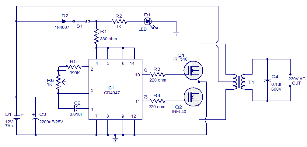
Custom Search

Wednesday, September 29, 2010

Vibration Sensor/Detector


With the help of a simple ceramic piezo-electric detector it is possible to assemble an interesting and useful Impact sensor unit,which can be used to detect impact and vibration on doors, showcases, windows etc. The shock sensor (Ceramic piezo-electric detector) uses a “unimorph” diaphram, which consists of a piezo-electric ceramic disk laminated to a metal disk. 


The sensor supplies a voltage proportional to the acceleration of the impact or vibration, for example 40mV/G ie output is near 2V for 60G impact.Here a low voltage, low current Impact sensor unit is realised using a standard ceramic piezo-electric detector which drives a monostable multivibrator (IC1) circuit to activate a npn silicon transistor (T1). Open collector output of this transistor switch can be interfaced to an external alarm/switch circuit for further processing. Since current consumption of the circuit is very low (from 5 to 6 mA only) any common 3V button cell can be used to power the sensor unit.When an impact is sensed, the monostable drives the transistor switch to ON , for a finite duration determined by the incircuit values of RC timing components R3 and C2.


The M74HC123 (IC1) is an high speed DUAL retriggerable CMOS MONOSTABLE MULTIVIBRATOR (MMV) fabricated with silicon gate C2MOS technology, with all inputs protected against static discharge and transient excess voltage. There are two trigger inputs, negative edge and positive edge. Here, only one monostable part with positive edge triggering (pin 2) is used. After triggering, the output maintains the monostable state for the time period determined by the external resistor R3 and capacitor C2.


Ref:www.electroschematics.com

7805 Regulator IC Circuits


Fixed voltage Positive and Negative regulator ICs are used in circuits to give precise regulated voltage.78 XX series regulator IC can handle maximum 1 ampere current. The Regulator ICs require minimum 1.5 higher input voltage than their voltage rating. For example 7805 IC requires minimum 6.5 volts to give 5 volt output. Here are some circuit designs of IC 7805 to monitor the output voltage.
1.This is the manipulation of the Regulator IC 7805 to give 9 volt regulated output. Normally the pin2 of the regulator IC is connected to the ground. Here it is connected to a 3.9 volt Zener diode. So the output from the Regulator IC will be 9 volts. 

2. This circuit can tell whether the IC 7805 is giving output or not. IC 7805 requires minimum 6.5 volt input to give 5 volt regulated output. When the input voltage is above 6.5 volts, Zener conducts and LED turns on indicating sufficient input voltage. Diffuse type Red LED requires 1.8 volts and Zener 4.7 volts .So to activate both these, input voltage should be minimum 6.5 volts. If the input voltage drops below 6.5 volts, Zener cutoff and LED turns off. This indicates the zero output from the regulator IC.
 3. This is a simple LED monitor to tell the output voltage from 7805. If the input voltage is above 6.5 volts, LED shows full brightness. When the input voltage reduces below 6.5 volts, brightness of LED decreases.
 D.Mohankumar

Tuesday, September 28, 2010

Wind-powered battery charger

In this wind-powered battery charger circuit the dc motor is used as a generator. The voltage output is proportional to its rpm. The LTC1042 monitors the voltage output and provides the following control function.


1. if the voltage output is below 13.8V, the control circuit is active and the NiCad battery is charging through the LM334 current source. The lead-acid battery is not being charged.
2. if the voltage output is between 13.8V and 15.1V, the 12V lead-acid battery is being charged at about 1-amp/hour rate (limited by the power FET).
3. if generator voltage exceeds 15.1V (a condition caused by excessive wind speed or when the 12V battery is fully charged), the a fixed load is connected, which limits the generator rpm to prevent damage.

This wind powered charger can be used as a remote source of power where wind energy is plentiful, such as on sailboats or at remote radio repeater sites. Unlike solar-powered panels, this system will function in bad weather and at night.
Battery Charger Schematic using wind energy

DIY Digital Thermometer

This diy digital thermometer circuit can measure temperatures up to 150°C with an accuracy of ±1°C. The temperature is read on a 1V full scale-deflection (FSD) moving-coil voltmeter or digital voltmeter.


 How the digital thermometer works

Operational amplifier IC 741 (IC3) provides a constant flow of current through the base-emitter junction of npn transistor BC108 (T1). The voltage across the base-emitter junction of the transistor is proportional to its temperature. The transistor used this way makes a low-cost sensor. You can use silicon diode instead of transistor.

The small variation in voltage across the base-emitter junction is amplified by second operational amplifier (IC4), before the temperature is displayed on the meter. Preset VR1 is used to set the zero-reading on the meter and preset VR2 is used to set the range of temperature measurement.

Operational amplifiers IC3 and IC4 operate off regulated ±5V power supply, which is derived from 3-terminal positive voltage regulator IC 7805 (IC1) and negative low-dropout regulator IC 7660 (IC2). The entire circuit works off a 9V battery.

Assemble the circuit on a general-purpose PCB and enclose in a small plastic box. Calibrate the thermometer using presets VR1 and VR2. After calibration, keep the box in the vicinity of the object whose temperature is
to be measured.

Digital Thermometer Circuit Schematic


Automatic Battery Charger


Here is a 12 volt Lead Acid battery charger that shut off the charging process once the battery attains full charge. This prevents overcharging of the battery so that, the charger can be left unattended. If the terminal voltage of the battery reduces below the set level, say 13.5 volts, the circuit automatically turns on to the charge mode.
Charging current as well as the power to the circuit is obtained from a 0-18 volt 2 Ampere step-down transformer. The low voltage AC is rectified by the bridge rectifier comprising D1 through D4 and made ripple free by the smoothing capacitor C1. For charging purpose, 18 volt DC is used while to power the circuit, 9 volt regulated DC from IC1 is used. IC2 (CA3140) is used as a simple voltage comparator to drive the relay. Its inverting input gets 4.7 volt reference voltage from the Zener ZD, while the non inverting input gets an adjustable voltage through the POT VR1.So normally, the inverting input pin 2 gets higher voltage from the Zener (as adjusted by VR1) and output of IC2 remains low. T1 then remains off keeping the relay off. The charging current passes to the battery through the NC (Normally Connected) contacts of the relay. When the terminal voltage of the battery increases to 13.5 volts, pin 3 of IC2 gets higher voltage than pin2 and the output of IC2 becomes high. This activates the relay and the contacts break. Charging current to the battery cut off and the relay remains as such since the battery voltage(13.5V or more) keeps the voltage at pin3 of IC2 is higher than that of pin 2.
Automatic Battery Charger Circuit

Setting: Before connecting the battery, set the input voltage to IC2 using a fully charged battery or variable power supply. Turn the switch S1 to the off position and switch on the power. Then connect a fully charged battery/ variable power supply to test points TP observing polarity. Measure the input voltage to pin 3 of IC2.Slowly adjust VR1 till the input voltage to pin 3 of IC2 raises to 5 volts. At this point, relay should energize and Red LED turns on. Then connect the battery for charging and switch on S1. If the battery takes charge, current to pin 3 of IC2 will be low since most of the current drain occurs into the battery. This keeps the relay off. When the battery voltage increases above 13.5 volts, no more current passes into the battery, so that the voltage at pin3 of IC2 rises and relay turns on.
D.Mohankumar

3 channel RF remote control

This is a 3 channel RF remote control project.The transmitter powered by 3V battery(coin size) range about 10 m.
Transmitter
This remote control I use PIC12F509 from Microchip which is a 8-pin single-chip microcontroller designed for low pin count applications with 1 K words flash memory and 41Byte SRAM and some special features such Power-saving Sleep mode,Wake-up from Sleep on pin change.


The RF transmitter module for this project is TLP434A(433.92MHz) which is an Ultra Small Wireless Transmitter is ideal for remote control projects or data transfers to a remote object.This compact unit operates from only 2V up to 12V but I choose 3V for compact size
remote control in this project . A range of up to 200m is possible with an antenna fitted and 12V battery are used.This module can works directly with HT12D or similiar decoder
To reduce the standby power and extend battery life I implement by putting the PIC12F509 microcontroller into SLEEP mode for most of the time and wake-up only when a key is pressed.The standby current I measured about 100nA in sleep mode.and about 14 mA when any switch pressed.
The diode D1 and D2 is implementing ground for TLP434A when any switch pressed.Thus there are no current drawn by TLP434A when it is in standby mode.
 Receiver
The RLP434A which is a Compact Radio Receiver(RF) works directly with the TLP434A transmitter on an operating frequency of 433.92MHz.Ideal for many applications, including robots, where commands can be sent directly to the robot, without the need for a hard-wired connection. Suitable for data rates of up to 4.8KHz, and the typical operating current is only 4.5mA.

RS232 transceiver circuits


There are serveral rs232 transceiver circuit which commond used for communicated between microcontroller and other devices such PC or any devices that use rs232.Here is a collection of rs232 transceiver circuits that popular for today.
The circit below use 2 transistor and some components to provide RS232 transceiver.It usefull for cheap application that dose not long lenght.
 MAX232(Full duplex)
The circuit below use MAX232 which is the MAXIM's devices.This circuit is very stable and use for professional design. This device is inexpensive and it can provides 2 channel for RS232 .
The MAX232 line drivers/receivers are designed for RS-232 and V.28 communications in harsh environments. Each transmitter output and receiver input is protected against ?15kV electrostatic discharge (ESD) shocks, without latchup.It can operate from a Single +5V Power Supply.
 DS275(Half Duplex)
This RS232 transceiver circuit use DS275 which is a small half duplex transceiver chip.I Compatible with RS–232–E signals and suitible for Low–power serial transmitter/receiver for battery-
backed application.Requies no external devices.

Simple DC power delay circuit


 The circuit diagram shown here is of a simple DC power delay circuit that is based on an SCR. This circuit is a very handy one and can be employed in many applications. The working of this circuit is very simple. When the input power is applied the capacitor C2 charges through resistor R2 and when the voltage across the capacitor just exceeds the Zener diode D3’s breakdown voltage, it breaks down and the SCR H1 is triggered and the delayed power will be available at the delayed OUT terminal.

Sunday, September 26, 2010

How an Inverter works.


Inverter.
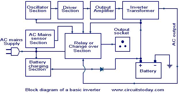
An inverter is used to produce an un-interrupted 220V AC or 110V AC (depending on the line voltage of the particular country) supply to the device connected as the load at the output socket.The inverter gives constant AC voltage at its output socket when the AC mains power supply is not available.
Lets look how the inverter makes this possible.To grasp the functioning of an inverter,we
should consider in the following situations.

* When the AC mains power supply is available.
* when the AC mains power supply is not available.
When the AC mains power supply is available.
When the AC mains supply is available,the AC mains sensor senses it and the supply goes to the Relay and battery charging section of the inverter.AC main sensor activates a relay and this relay will directly pass the AC mains supply to the output socket.The load will by driven by the line voltage in this situation.Also the line voltage is given to the battery charging section where the line voltage is converted to a DC voltage(12V DC or 24V DC usually),then regulated and battery is charged using it.There are special circuits for sensing the battery voltage and when the battery is fully charged the charging is stopped.In some inverters there will be a trickle charging circuit which keeps the battery constantly at full charge.

When the AC mains power supply is not available.

When the AC mains power supply is not available,an oscillator circuit inside the inverter produces a 50Hz MOS drive signal.This MOS drive signal will be amplified by the driver section and sent to the output section.MOSFETs or Transistors are used for the switching operation.These MOSFETs or Transistors are connected to the primary winding of the inverter transformer.When these switching devices receive the MOS drive signal from the driver circuit,they start switching between ON & OFF states at a rate of 50 Hz.This switching action of the MOSFETs or Transistors cause a 50Hz current to the primary of the inverter transformer.This results in a 220V AC or 110V AC (depending on the winding ratio of the inverter transformer) at the secondary or the inverter transformer.This secondary voltage is made available at the output socket of the inverter by a changeover relay.
Automation in an Inverter.
Inverter contains various circuits to automatically sense and tackle various situations that may occur when the inverter is running or in standby.This automaton section looks after conditions such as overload,over heat,low battery,over charge etc.Respective of the situation, the automation section may switch the battery to charging mode or switch OFF.The various conditions will be indicated to the operator by means of glowing LEDs or sounding alarms.In advanced inverters LCD screens are used to visually indicate the conditions.


Using inverters with AC generators.


Inverter systems can be in-corporated with generator systems to attain longer run-time when there is a cut in the mains power supply.The essential and critical loads require undisturbed power supply when the mains AC power supply falls for extended periods.The inverter can be used to power the critical and essential loads when the power supply fails.The generator can be started automatically or manually when the power cut extends for longer periods and the inverter battery becomes exhausted.In such a condition the inverter alone cannot provide necessary to the loads.
Instead of drawing power from the battery,the inverter draws power from the generator and continues to power the critical loads.In such a configuration the run time of the inverter will not be affected by the capacity of the battery.The extended run time can be also achieved by using extra batteries.But this method proves to be more costly and space consuming.Also unlimited run time cannot be attained by using extra batteries.
An inverter which is backed up by an AC generator is one of the most easy method to produce a power protection for prolonged time at minimum cost.Also the generator must be selected such that it can handle the effects of sudden changes in the load.The common habit is to use a generator with a rating of around 6 to 8 times that of the load.As an example a generator of 8KVA can be used for a house drawing 1KVA power.This could prevent a lot of problems associated with the generator as well as inverter.Also special care must bu taken to assure that the inverter will function properly with the AC generator.The common scheme for connecting an inverter with a generator is shown below.

100W inverter circuit


Here is the circuit diagram of a simple 100 watt inverter using IC CD4047 and MOSFET IRF540. The circuit is simple low cost and can be even assembled on a veroboard.CD 4047 is a low power CMOS astable/monostable multivibrator IC. Here it is wired as an astable multivibrator producing two pulse  trains of 0.01s which are 180 degree out of phase at the pins 10 and 11 of the IC.

Pin 10 is connected to the gate of Q1 and pin 11 is connected to the gate of Q2. Resistors R3 and R4 prevents the loading of the IC by the respective MOSFETs. When pin 10 is high Q1 conducts and  current flows through the upper half of the transformer primary which accounts for the positive half of the output AC voltage. When pin 11 is high Q2 conducts and  current flows through the lower half of the transformer primary in opposite direction and it accounts for the negative half of the output AC voltage.

Notes.
  • B1 can be  a 12V/ 6Ah lead acid battery.
  • Q1 and Q2 must be fitted to a proper heat sink.
  • T1 can be a 9-0-9 V primary, 230V secondary, 150VA transformer .
  • Do not expect much from this circuit. The is very simple one suitable for low grade applications.

Read more: http://www.circuitstoday.com/category/inverters-ups#ixzz10hrfoWk6


Level Switch


 Here is a simple level switch circuit that switches on one relay and switches off another relay when the fluid level exceeds the set limit.This circuit is a modification of the “Simple Water Level Indicator” previously posted.When the water level touches the probes positive supply is connected to the base of Q1 through fluid.This makes transistor Q1 ON.Base of Q2 is connected to collector of Q1 and base of Q3 is connected to collector of Q2.As a result Q1 will be on and Q2 will be OFF.So K2 will be OFF and K1 will be ON.Net result, we get two relays operating according to level ,one ON and Other OFF.The contacts of the relays OP1 and OP2 can be used according to your need to operate any device like motor,pumps,solenoid valves,light,alarm etc.When water level falls K2 will be ON and K1 will be OFF.
Notes
  • Adjust R1 keeping probes touched in water to obtain the relay K1 ON.Then remove probes from water and see relay K1 goes OFF.During this time the opposite will be happening in K2.If you cannot attain the setting replace R1 with a 500K POT and repeat the procedure.That’s enough.
  • For the probes cut 2 1 sqcm aluminum sheets and connect it to good quality insulated Aluminum wires. 2 cm spacing between probes is enough.Mount the two probes parallely at the desired level.Circuit is ready.
  • One problem of this circuit is the corrosion of probes since DC is used.Any way this setup will run problem free for at least one year. We are developing a corrosion free version of the same circuit.That will be here soon.


Read more: http://www.circuitstoday.com/level-switch#ixzz10hq9cnx3
Under Creative Commons License: Attribution


Temperature controlled DC fan


Here is a simple circuit based on two transistors that can be used to control the speed of a 12 V DC fan depending on the temperature.A thermistor (R1) is used to sense the temperature. When the temperature increases the base current of Q1 (BC 547) increases which in turn decreases the collector voltage of the same transistor. Since the collector of Q1 is coupled to the base of Q2 (BD 140), the decrease in collector voltage of Q1 forward biases the Q2 more and so do the speed of the motor. Also, the brightness of the LED will be proportional to the speed of the motor.

PWM Motor Speed Control Circuit


 Here is a simple PWM motor speed controller circuit that can be used for varying the speed of low power DC motors .The variation in speed is achieved by varying the duty cycle of the pulse supplied to drive the motor.Of the two gates of IC CD40106B ,N1 is wired as an inverting Schmitt Trigger astable multi vibrator for producing pulses and N2 as an inverting buffer to drive the transistor during positive cycles at base.The duty cycle is set from resistor R2. R1 limits the base current of transistor SL 100.The circuit is ideal for controlling toy motors,hand held mini fans , small blowers etc.

200M FM Transmitter


 A very stable and simple FM transmitter circuit is given here. With a matching antenna, this transmitter can attain a range of around 200 meters. I assembled this transmitter few years and got very good results. Let us see how the circuit works.
A condenser microphone (K1) is used to pick the sound to be transmitted. Capacitor C1 is a DC decoupler and the sound signal is coupled to the base of Q1 which wired as a preamplifier.R2 and R3 are the biasing resistors of Q1. Amplified sound signal will be available at the collector of Q1 and it coupled to the emitter of transistor Q2 through the capacitor C4 and 1mH inductor L1. Capacitor C4 decouples the DC component from the preamplifier output. Q2 performs the job of oscillator and modulator. Inductor L2 and variable capacitor C5 forms the tank circuit necessary for creating oscillations. Capacitor C6 is the feedback capacitor. The modulated FM wave will be available at the collector of Q1 and it is transmitted using the antenna A1.

2 km FM transmitter


With a matching antenna,the FM transmitter circuit shown here can transmit signals up to a range of 2 kilo meters. The transistor Q1 and Q2 forms a classic high sensitive preamplifier stage.The audio signal to be transmitted is coupled to the base of Q1 through capacitor C2. R1, R3, R4, R6, R5 and R9 are the biasing resistors for the preamplifier stage comprising of Q1 and Q2. Transistor Q3 performs the collective job of oscillator, mixer and final power amplifier.C9 and L1 forms the tank circuit which is essential for creating oscillations. Inductor L2 couples the FM signal to the antenna.


Notes.
  • Assemble the circuit on a good quality PCB.
  • The circuit can be powered from anything between 9 to 24V DC.
  • Inductor L3 can be a VK220J type RFC.
  • For L1 make 3 turns of 1mm enamelled copper wire on a 10mm diameter plastic former. On the same core make 2 turns of 1 mm enamelled copper wire close to L3 and that will be L2.
  • Frequency can be adjusted by varying C9.
  • R9 can be used to adjust the gain.
  • For optimum performance, value of C8 must be also adjusted.
  • Using a battery for powering the circuit will reduce noise.

http://www.circuitstoday.com/2-km-fm-transmitter#ixzz10eBAERgs


Voltage doubler circuit using NE555


The circuit diagram of a very simple voltage doubler using NE555 timer is shown here. Here IC NE555 The negative terminal of the capacitor C3 will be shorted to ground through T2 and it will be charged to the input supply voltage. When the output of the astable multi vibrator is high, transistor Q1 will be ON and transistor Q2 will be OFF. The capacitor C4 will be charged to the voltage across capacitor C3 plus the input supply voltage (that is double the input voltage). This is how the circuit works.


This voltage doubler circuit can deliver only up to 50mA output current and above that current limit the output voltage will be dramatically reduced. The actual output voltage will be around 19V for a 12V DC input and also the output voltage will be a bit unstable. Anyway, for low current applications this circuit is well enough.

Saturday, September 25, 2010

Single Chip FM Radio circuit


Here is a compact low cost FM radio circuit using IC7400. This circuit is designed as per the data sheet and the result is excellent.Ideal for all category of electronic enthusiasts.
The TDA7000 is a monolithic integrated circuit for mono FM portable radios, where a minimum on peripheral components is crucial. The IC TDA 7000 has a Frequency-Locked-Loop system with an intermediate frequency of 70 kHz. The intermediate frequency selectivity is achieved by active RC filters. The only function which needs alignment is the resonant circuit for the oscillator, thus selecting the reception frequency. Spurious reception is avoided by means of a mute circuit, which also eliminates too noisy input signals. Special steps are taken to meet the radiation requirements.


24W amplifier using TDA1516


 Here is the circuit diagram of a simple 24W mono amplifier using IC TDA1516.The TDA1516 is an integrated class B power amplifier in a 13 pin SIL package. The IC has many useful features such as short circuit protection, load dump protection, thermal protection, reverse polarity protection etc. Here the IC is wired in BTL mode to deliver 24W of power into a 4 ohm speaker. This amplifier can be operated from a 12V DC supply and this makes it suitable for car audio applications. 


AM receiver circuit


 Here is a low cost AM receiver circuit that can be tuned from around 550 to 1100 KHz. Three transistors are used in this project. The transistors Q1 and Q2 are wired as a compound transistor pair in which Q1 is an emitter follower and Q2 is a common emitter amplifier. The emitter follower prevents the loading of tank circuit, while the common emitter amplifier necessary voltage gain. The L1 and C2 forms the tank circuit.The L1 also does the job of antenna.The series combination of R6 and R7 gives a regenerative feedback between output of the Q2 and tank circuit. The transistor Q3 performs the demodulation of the carrier signal. It also provides amplification the demodulated signal. The audio output is coupled out from the collector of Q3 via the capacitor C3.Capacitor C6 provides some noise filtering.

AM Transmitter circuit


 Here is the circuit diagram of a simple AM transmitter circuit that can transmit your audios to your backyard.This circuit is designed with limited the power output to match the FCC regulations and still produces enough amplitude modulation of voice in the medium wave band to satisfy your personal needs.You will love this!.
The circuit has two parts , an audio amplifier and a radio frequency oscillator. The oscillator is built around Q1 (BC109) and related components. The tank circuit with inductance L1 and capacitance VC1 is tunable in the range of 500kHz to 1600KHz. These components can be easily obtained from your old medium wave radio. Q1 is provided with regenerative feedback by connecting the base and collector of Q1 to opposite ends of the tank circuit. C2 ,the 1nF capacitance , couples signals from the base to the top of L1, and C4 the 100pF capacitance ensures that the oscillation is transfered from collector, to the emitter, and through the internal base emitter resistance of the transistor Q2 (BC 109) , back to the base again. The resistor R7 has a vital part in this circuit. It ensures that the oscillation will not be shunted to ground trough the very low value internal emitter resistance, re of Q1(BC 109), and also increases the input impedance such that the modulation signal will not be shunted to ground. Q2 is wired as a common emitter RF amplifier, C5 decouples the emitter resistance and unleashes full gain of this stage. The microphone can be electret condenser microphone and the amount of AM modulation can be adjusted by the 4.7 K variable resistanceR5.

Friday, September 24, 2010

Infrared motion detector circuit


Here is the circuit diagram of an infrared motion detector that can be used to sense intrusions.Infra red rays reflected from a static object will be in one phase, and the rays reflected from a moving object will  be in another phase.The circuit uses this principle to sense the motion.
The IC1 (NE 555)  is wired as an astable multivibrator .The IR diode connected at the
output of this IC produces infrared beams of frequency 5Khz.These beams are picked by the photo transistor Q1 .At normal condition ie; when there is no intrusion the output pin (7) of IC2 will be low.When there is an intrusion the phase of the reflected waveforms has a difference in phase and this phase difference will be picked by the IC2.Now the pin 7 of the IC 2 goes high to indicate the intrusion.An LED or a buzzer can be connected at the output of the IC to indicate the intrusion.


Schmitt Trigger using Op-Amp


A Schmitt trigger circuit is a fast-operating voltage-level detector. When the input voltage arrives at the upper or lower trigger levels, the output changes rapidly. The circuit operates with almost any type of input waveform, and it gives a pulse-type output.The circuit of an op-amp Schmitt trigger circuit is shown in figure. 


The input voltage vin is applied to the inverting input terminal and the feedback voltage goes to the non-inverting terminal. This means the circuit uses positive voltage feedback instead of negative feedback, that is, in this circuit feedback voltage aids the input voltage rather than opposing it. For instance, assume the inverting input voltage to be slightly positive. This will produce a negative output voltage. The voltage divider feedsback a negative voltage to the non-inverting input, which results in a larger negative voltage. This feedsback more nega tive voltage until the circuit is driven into negative saturation. If the input voltage were, slightly negative instead of positive, the circuit would be driven into the positive saturation. This is the reason the circuit is also referred to as re generative comparator.

Full wave bridge rectifier


In the bridge circuit four diodes are connected in the form of a Wheatstone bridge, two diametrically opposite junctions of the bridge are connected to the secondary of a transformer and the other two are connected to the load.When the upper end of the transformer second ary winding is positive, say during first half-cycles of the input supply, diodes D1 and D3 are forward biased and current flows through arm AB, enters the load at positive terminal, leaves the load at negative termi nal, and returns back flowing through arm DC.

 Dur ing this half of each input cycle, the diodes D2 and D4 are reverse biased and so the current is not allowed to flow in arms AD and BC. The flow of current is indicated by solid arrows in the figure. In the second half of the input cycle the lower end of ac supply becomes positive, diodes D,2 and D4 become forward biased and current flows through arm CB, enters the load at the positive terminal, leaves the load at nega tive terminal and returns back flowing through arm DA. Flow of current has been shown by dotted ar rows in the figure. Thus the direction of flow of cur rent through the load resistance RL remains the same during both half^eycles of the input supply voltage.


Air flow detector circuit.


This circuit can give a visual indication of the rate of air flow.It can be also used to check whether there is air flow in a given space.The filament of a incandescent bulb is the sensing part of the circuit.When there is no air flow the resistance of the filament will be low.When there is air flow the resistance drops , because the moving air will remove some of the heat generated in the filament.This variations in the resistance will produce variation of voltage across the filament.These variations will be picked up by the opamp (LM339) and the brightness of the LED at its output will be varied proportionally to the airflow.


Notes.
  • The filament L1 can be made by removing  the glass of a 40W incandescent bulb.
  • The circuit can be powered from a 12 V DC power supply.
Read more: http://www.circuitstoday.com/air-flow-detector-circuit#ixzz10TGQRPqM

10V switching regulator using LM5007


 The circuit diagram shown here is of a 10V switching regulator based on the LM5007 from National Semiconductors. The LM5007 is an integrated step down switching regulator which has all necessary systems required for making a cost effective and reliable switching regulator circuit. The IC is available in MSOP-8, LLp-8 packages and has a lot of built in features like thermal shut down, under voltage lock out, duty cycle limiting, current limiting etc.The output voltage of this regulator can be adjusted using the resistor R3 and R4. For the given values of R3 and R4 in the circuit diagram, the output voltage will be 10V. The equation governing the output voltage is Vout = 2.5 x (R3+R4)/R4. Resistor R1 sets the switch on time and C4 is the boost boot strap capacitor. Resistor R2 determines the variation of OFF time and C3 is a decoupling capacitor.
Notes.
  • The supply voltage can be anything between 12 to 72V DC.
  • Output voltage can be adjusted using R3 and R4.
  • C1  and C5 are polyester capacitors.
  • C1 and C2 must be rated at least 100V.
  • R5 and C5 forms a filter network.
  • The output current limit of LM5007 is 700mA.


Read more: http://www.circuitstoday.com/category/power-supplies#ixzz10TExkBTK
Under Creative Commons License: Attribution

Analog PID Controller


The circuit diagram below shows us about a form of PID controller. The input signal is buffered and amplified by a non-inverting amplifier and the gain of this stage defines the proportional gain P of the controller.The amplified error signal passes in parallel through an integrator (top) a unity-gain amplifier (middle) and a differentiator (bottom) all of which have inverting behaviour. The final op-amp sum and invert the outputs and passed to the output.  
The potentiometers labeled D and I control the proportions in which derivative and integral fractions contribute to the output signal which is proportional to the power W to be supplied to the heater.t is most likely to be troublesome by causing an offset between the set-point and oven temperatures.
Under some circumstances the integrator may drift and eventually saturate which would prevent it from working properly. To reduce the impact of op-amp offset and bias, the first thing to try would be a resistor, equal in value to R2, between the positive input of the integrating op-amp and ground to eliminate the common-mode bias current. Selecting an op-amp with a good input-offset performance would be the next step.

Light detector using a relay


Following circuit is same as the above mentioned dark detector. In this case, the configuration of relay has been changed. Now, NO (Normally open) terminal has been left open. In normal case, the D1-LED remains ON. When light falling on LDR is interrupted, pole of relay connects to NO terminal. Hence, NC (Normally connected) terminal does not get power and that switches the D1- LED off.

Dark detector using a relay


Circuit given below is an automatic dark detector. When light falling on LDR gets interrupted, RL1- 6Vrelay becomes active, pole gets connected with NO(Normally Open) terminal of relaand D1-LED gets power through resistance R2-470R.

Thursday, September 23, 2010

4-Channel Commutator


To reach low channel ON resistance (<30 Ohm) and low OFF current leakage, 4-channel commutator uses the 2N4091. The DM7800 voltage translator is a monolithic device. This device give us +10V to -20V gate drive to the JFETs while at the same time giving DTL-TTL logic compatibility.

Here’s the circuit diagram:


Closed-Loop Automatic Power Control for RF Applications


This is a circuit of Closed-Loop Automatic Power Control for RF Applications. The circuit uses a log detector (AD8318) and a VGA (ADL5330). This circuit has a high temperature stability because of the high temperature stability of the AD8318. The AD8318 also ensures the same level of temperature stability at the output of the ADL5330 VGA. The ADL5330 is converted from an open-loop variable gain amplifier into a closed-loop output power control circuit by the log amp detector. The POUT vs. setpoint transfer function of AD8318 follows a linear-in-dB characteristic because the AD8318 has a linear-in-dB transfer function. Here is the circuit:

A sample of the output RF must be fed back to the detector by using additional attenuation and a directional coupler to operate the ADL5330 VGA in an AGC loop. A DAC is used to apply A setpoint voltage to the VSET input of the detector. The VOUT is connected to the GAIN pin of the ADL5330. The GAIN voltage is adjusted by the detector until the level at the RF input corresponds to the applied setpoint voltage. The correct balance between the setpoint voltage and the input signal level at the detector is set by the GAIN. [Source: Analog Devices Application Note]

555 IC Linear Ramp (Sawtooth) Generator/Oscillator


The Vc1 increases linearly when the pull-up resistor RA in the monostable circuit is replaced with constant current source, generating a linear ramp. The linear ramp generating circuit and the generated linear ramp waveforms illustration is shown in figures below.


Ic= (Vcc-Ve)/Re
Ve= Vbe + (R2/(R1+R2))Vcc
For example, if Vcc=15V, RE=20k, R1=5kW, R2=10k, and VBE=0.7V, VE=0.7V+10V=10.7V, Ic=(15-10.7)/20k=0.215mA
The current flowing through capacitor C1 becomes a constant current generated by PNP transistor and resistor when the trigger starts in a timer configured as shown in figure below.
Hence, the Vc is linear function. The gradient S of the linear ramp function is defined as:
S= (Vp-p)/T
The Vp-p is the peak to peak voltage. The Vc comes out as follows is the electric charge amount accumulated in the capacitor is divided by the capacitance.
V= Q/C
The above equation divided on both sides by T gives us
V/T= (Q/T)/C
and may be simplified into the following equation.
S=I/C
In other words, we can obtained the gradient of the linear ramp function appearing across the capacitor by using the constant current flowing through the capacitor. The gradient of the ramp function at both ends of the capacitor is S = 0.215m/0.022? = 9.77V/ms if the constant current flow through the capacitor is 0.215mA and the capacitance is 0.02uF. [Circuit's schematic diagram source: Philips Semiconductors Application Notes]

PID Controller Using Op-Amp


Generally, specifically combined ICs perform a control task. We can carry out simple controls using analog ICs, such as operational amplifier circuitry. The basic component of “Control Electronics” is an integrated circuit (IC). IC is a small electronic device made out of a semiconductor material.According to equation 1, this analog circuit calculates PID control response. Sensor signal VIN is amplified by IC1 (P mode), integrated by IC2 (I mode), and differentiated by IC3 (D mode), and all three modes are summed by IC4 to derive control response VOUT


[Source: Jeon and Chun]

Sunday, September 19, 2010

Strain gage Amplifier


Form on the left is the amplifier PCB Stain Gage can measure up to two channels through integrated bridge circuit to detect changes in resistance. When loaded action allows the stain gage resistance to change, so will the bridge circuit imbalance with the relationship. Eo / Ei = Rg2 / (Rg2 R)-Rg1 / (Rg1 R) and use changes, the pressure is used to amplify signals with the INA129 or INA 2126P when the amplifier and then put the LPF to eliminate signals that are not needed. out that in this 10Hz cut off frequency and then the adjustment to the DC-offset voltage can be adjusted to start at the center or at the time. And will then be issued to signal Vo, such as Digital Signal Processing and DAQ or Micro controller be contacting the Rs-232.

Labview rs232


Rs232 is a communication between Hardware and Software can be applied in measurement such as Data-Logger The Software has many led to writing, such as Labview ni we use ni as a receptor for the Hardware because they can write. No matter how small it is easy to program graphic Language and Hardware for PIC Micro controller family by writing to the PIC program to send and receive data between the Hw / Sw and the information obtained to be graphed, or stored in Lab tops.In general, job monitoring various vital that we want to bring up the display, whether to a Personal computer or LCD displays various reasons, we want to bring that information to store and brought forth. Analysis later. In this section we will discuss implementation of the inspection data to knowledge (Sensor) through the Micro Controller to display a Program labview using the receiver. When the first step and open up to the block diagram-> Instrument I / O -> Serial then block the following name.1.configure Port.2.Read.3.Clode.Values that have come out that the data is still of type String, we are able to convert to Double the number to be displayed as waveform graph.