Custom Search

Sunday, October 17, 2010

Electronic Thermostat

Mechanical thermostat has been around for a long time and has been used in industrial control, home appliances control and many other devices to measure and control the temperature of a certain processes. The sensor used usually is a bimetallic sensor that is make from two different metals that expand at different rates as they are heated up. These metal strips arebonded together and when the temperature rises, the strips will bend upward hence making connection to the contact of thecircuit so that current can flow through the circuit.
As the temperature cools down, it will go back to its original positionand disconnect the current from the circuit. By adjusting the strip and the contact, the temperature can be contolled. Mostoven and air conditioners use this type of sensor. The mechanical thermostat is more widely used due to its lower cost compared to electronic thermostat.
The use of electronic thermostat is becoming more popular now as the cost of semiconductor continues to drop with the advancement of better fabrication and packaging processes. Many applications have switched to electronic control as thecontrol of the temperature is more accurate, easier to control the desired temperature using digital technology, more reliable and interfacing with other devices.
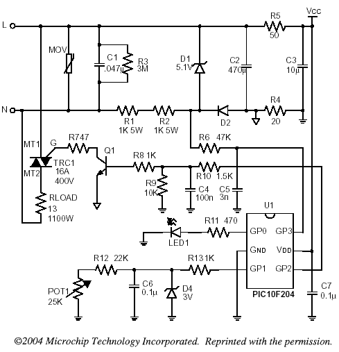
This application note from Microchip uses a low cost 6 pin microcontroller in the design of electronic thermostat. Thefeatures of PIC10F204 are as shown below. One advantage is that it has the PDIP package which makes it easier for electronichobbyists to do their own soldering.
  • 256 Words Program Memory and 16 bytes Static RAM
  • Wide Operating Voltage from 2.0V to 5.5V DC
  • 3 I/O
  • 1 comparator
  • 25 mA source/sink current I/O
  • 1 8-bit timers.
 
Among the learning experiences one gained from this projects are:
  • Power supply is directly tapped from the AC lines voltage using a resistive based power supply. This makes the entirecircuit live and one has to be careful when implementing this project. Ensure that no parts of the circuit is accessible toany user. Use a plastic enclosure to house the printed circuit board properly.
  • The principles of triac is briefly discussed here. The use of zero crossing detection is useful as many applicationsuse this method in their operations. Among them are light dimmer and motor control applications.
  • Learn how to optimise the program code to make it efficient. Many programmers use long routines to accomplish a certaintask when a few lines of codes would be sufficient. This experience needs to be learned as one hands on a project and repeatedly look into the code to make it shorter and efficient.
  • Having learned the code, one can then modify and add temperature sensor to make it a close loop control. Display circuity and user interface can be added to the system by migration to a higher pin count microcontroller.
The full application note and source code of the Microcontroller Based Electronic Thermostat Project can be obtained from Microchip website.
 
http://www.electronics-project-design.com/ElectronicThermostat.html

Cheap 12V to 220V Inverter

Even though today’s electrical appliances are increasingly often self-powered, especially the portable ones you carry around when camping or holidaying in summer, you do still sometimes need a source of 230 V AC - and while we’re about it, why not at a frequency close to that of the mains? As long as the power required from such a source remains relatively low - here we’ve chosen 30 VA - it’s very easy to build an inverter with simple, cheap components that many electronics hobbyists may even already have.
Cheap 12V to 220V Inverter Circuit Schematic
Though it is possible to build a more powerful circuit, the complexity caused by the very heavy currents to be handled on the low-voltage side leads to circuits that would be out of place in this summer issue. Let’s not forget, for example, that just to get a meager 1 amp at 230 VAC, the battery primary side would have to handle more than 20 ADC!. The circuit diagram of our project is easy to follow. A classic 555 timer chip, identified as IC1, is configured as an astable multivibrator at a frequency close to 100 Hz, which can be adjusted accurately by means of potentiometer P1.As the mark/space ratio (duty factor) of the 555 output is a long way from being 1:1 (50%), it is used to drive a D-type flip-flop produced using a CMOS type 4013 IC. This produces perfect complementary square-wave signals (i.e. in antiphase) on its Q and Q outputs suitable for driving the output power transistors. As the output current available from the CMOS 4013 is very small, Darlington power transistors are used to arrive at the necessary output current. We have chosen MJ3001s from the now defunct Motorola (only as a semi-conductor manufacturer, of course!) which are cheap and readily available, but any equivalent power Darlington could be used.These drive a 230 V to 2 × 9 V center-tapped transformer used ‘backwards’ to produce the 230 V output. The presence of the 230 VAC voltage is indicated by a neon light, while a VDR (voltage dependent resistor) type S10K250 or S07K250 clips off the spikes and surges that may appear at the transistor switching points. The output signal this circuit produces is approximately a square wave; only approximately, since it is somewhat distorted by passing through the transformer. Fortunately, it is suitable for the majority of electrical devices it is capable of supplying, whether they be light bulbs, small motors, or power supplies for electronic devices.
PCB layout:
PCB Layout Of Cheap 12V to 220V Inverter Circuit Schematic
PCB Layout For Cheap 12V to 220V Inverter Circuit Diagram
COMPONENTS LIST
Resistors
R1 = 18k?
R2 = 3k3
R3 = 1k
R4,R5 = 1k?5
R6 = VDR S10K250 (or S07K250)
P1 = 100 k potentiometer
Capacitors
C1 = 330nF
C2 = 1000 µF 25V
Semiconductor
T1,T2 = MJ3001
IC1 = 555
IC2 = 4013
Miscellaneous
LA1 = neon light 230 V
F1 = fuse, 5A
TR1 = mains transformer, 2x9V 40VA (see text)
4 solder pins
Note that, even though the circuit is intended and designed for powering by a car battery, i.e. from 12 V, the transformer is specified with a 9 V primary. But at full power you need to allow for a voltage drop of around 3 V between the collector and emitter of the power transistors. This relatively high saturation voltage is in fact a ‘shortcoming’ common to all devices in Darlington configuration, which actually consists of two transistors in one case. We’re suggesting a PCB design to make it easy to construct this project; as the component overlay shows, the PCB only carries the low-power, low-voltage components.
The Darlington transistors should be fitted onto a finned anodized aluminum heat-sink using the standard insulating accessories of mica washers and shouldered washers, as their collectors are connected to the metal cans and would otherwise be short-circuited. An output power of 30 VA implies a current consumption of the order of 3 A from the 12 V battery at the ‘primary side’. So the wires connecting the collectors of the MJ3001s [1] T1 and T2 to the transformer primary, the emitters of T1 and T2 to the battery negative terminal, and the battery positive terminal to the transformer primary will need to have a minimum cross-sectional area of 2 mm2 so as to minimize voltage drop.
The transformer can be any 230 V to 2 × 9 V type, with an E/I iron core or toroidal, rated at around 40 VA. Properly constructed on the board shown here, the circuit should work at once, the only adjustment being to set the output to a frequency of 50 Hz with P1. You should keep in minds that the frequency stability of the 555 is fairly poor by today’s standards, so you shouldn’t rely on it to drive your radio-alarm correctly – but is such a device very useful or indeed desirable to have on holiday anyway? Watch out too for the fact that the output voltage of this inverter is just as dangerous as the mains from your domestic power sockets.
So you need to apply just the same safety rules! Also, the project should be enclosed in a sturdy ABS or diecast so no parts can be touched while in operation. The circuit should not be too difficult to adapt to other mains voltages or frequencies, for example 110 V, 115 V or 127 V, 60 Hz. The AC voltage requires a transformer with a different primary voltage (which here becomes the secondary), and the frequency, some adjusting of P1 and possibly minor changes to the values of timing components R1 and C1 on the 555.

http://www.extremecircuits.net/2010/05/cheap-12v-to-220v-inverter.html

4-Bit Analogue to Digital Converter

The operation of the converter is based on the weighted adding and transferring of the analogue input levels and the digital output levels. It consists of comparators and resistors. In theory, the number of bits is unlimited, but each bit needs a comparator and several coupling resistors. The diagram shows a 4-bit version. The value of the resistors must meet the following criteria:
  • R1:R2 = 1:2;
  • R3:R4:R5 = 1:2:4;
  • R6:R7:R8:R9 = 1:2:4:8.
The linearity of the converter depends on the degree of precision of the value of the resistors with respect to the resolution of the converter, and on the accuracy of the threshold voltage of the comparators. This threshold level must be equal, or nearly so, to half the supply voltage. Moreover, the comparators must have as low an output resistance as possible and as high an input resistance with respect to the load resistors as feasible. Any deviation from these requirements affects the linearity of the converter adversely. Circuit diagram:4-Bit Analogue to Digital Converter Circuit Diagram
If the value of the resistors is not too low, the use of inverters with an FET (field-effect transistor) input leads to a near-ideal situation. In the present converter, complementary metal-oxide semiconductor (CMOS) inverters are used, which, in spite of their low gain, give a reasonably good performance. If standard comparators are used, take into account the output voltage range and make sure that the potential at their non-inverting inputs is set to half the supply voltage. If high accuracy is a must, comparators Type TLC3074 or similar should be used. This type has a totem-pole output. The non-inverting inputs should be interlinked and connected to the tap of a a divider consisting of two 10 kΩ resistors across the supply lines. It is essential that the converter is driven by a low-resistance source. If necessary, this can be arranged via a suitable op amp input buffer. The converter draws a current not exceeding 5 mA.

http://www.extremecircuits.net/2010/07/4-bit-analogue-to-digital-converter.html

PIC Controlled Relay Driver

This circuit is a relay driver that is based on a PIC16F84A microcontroller. The board includes four relays so this lets us to control four distinct electrical devices. The controlled device may be a heater, a lamp, a computer or a motor. To use this board in the industrial area, the supply part is designed more attentively. To minimize the effects of the ac line noises, a 1:1 line filter transformer is used.
PIC Controlled Relay Driver
The components are listed below.
1 x PIC16F84A Microcontroller
1 x 220V/12V 3.6VA (or 3.2VA) PCB Type Transformer (EI 38/13.6)
1 x Line Filter (2x10mH 1:1 Transformer)
4 x 12V Relay (SPDT Type)
4 x BC141 NPN Transistor
5 x 2 Terminal PCB Terminal Block
4 x 1N4007 Diode
1 x 250V Varistor (20mm Diameter)
1 x PCB Fuse Holder
1 x 400mA Fuse
2 x 100nF/630V Unpolarized Capacitor
1 x 220uF/25V Electrolytic Capacitor
1 x 47uF/16V Electrolytic Capacitor
1 x 10uF/16V Electrolytic Capacitor
2 x 330nF/63V Unpolarized Capacitor
1 x 100nF/63V Unpolarized Capacitor
1 x 4MHz Crystal Oscillator
2 x 22pF Capacitor
1 x 18 Pin 2 Way IC Socket
4 x 820 Ohm 1/4W Resistor
1 x 1K 1/4W Resistor
1 x 4.7K 1/4W Resistor
1 x 7805 Voltage Regulator (TO220)
1 x 7812 Voltage Regulator (TO220)
1 x 1A Bridge Diode
The transformer is a 220V to 12V, 50Hz and 3.6VA PCB type transformer. The model seen in the photo is HRDiemen E3814056. Since it is encapsulated, the transformer is isolated from the external effects. A 250V 400mA glass fuse is used to protect the circuit from damage due to excessive current. A high power device which is connected to the same line may form unwanted high amplitude signals while turning on and off. To bypass this signal effects, a variable resistor (varistor) which has a 20mm diameter is paralelly connected to the input.
Another protective component on the AC line is the line filter. It minimizes the noise of the line too. The connection type determines the common or differential mode filtering. The last components in the filtering part are the unpolarized 100nF 630V capacitors. When the frequency increases, the capacitive reactance (Xc) of the capacitor decreases so it has a important role in reducing the high frequency noise effects. To increase the performance, one is connected to the input and the other one is connected to the output of the filtering part.
After the filtering part, a 1A bridge diode is connected to make a full wave rectification. A 2200 uF capacitor then stabilizes the rectified signal. The PIC controller schematic is given in the project file. It contains PIC16F84A microcontroller, NPN transistors, and SPDT type relays. When a relay is energised, it draws about 40mA. As it is seen on the schematic, the relays are connected to the RB0-RB3 pins of the PIC via BC141 transistors. When the transistor gets cut off, a reverse EMF may occur and the transistor may be defected.
To overcome this unwanted situation, 1N4007 diodes are connected between the supply and the transistor collectors. There are a few number of resistors in the circuit. They are all radially mounted. Example C and HEX code files are included in the project file. It energizes the next relay after every five seconds.

Read more:http://www.extremecircuits.net/2010/08/pic-controlled-relay-driver.html

CMOS Crystal Frequency Multiplier

Crystals usually operate at fundamental frequencies up to about 15 MHz. Whenever higher frequencies are required a frequency multiplier is placed after the crystal oscillator. The resulting output signal is then a whole multiple of the crystal frequency. Other frequency multipliers often use transistors, which produce harmonics due to their non-linearity. These are subsequently filtered from the signal. One way of doing this is to put a parallel L-C filter in the collector arm. This filter could then be tuned to three times the input frequency. A disadvantage is that such a circuit would quickly become quite substantial.

This circuit contains only a single IC and a handful of passive components, and has a complete oscillator and two frequency triplers. The output is therefore a signal with a frequency that is 9 times as much as that of the crystal. Two gates from IC1, which contains six high-speed CMOS inverters, are used as an oscillator in combination with X1. This works at the fundamental frequency of the crystal and has a square wave at its output. A square wave can be considered as the sum of a fundamental sine wave plus an infinite number of odd multiples of that wave. The second stage has been tuned to the first odd multiple (3 x).

We know that some of our readers will have noticed that the filter used here is a band-rejection (series LC) type. Worse still, when you calculate the rejection frequency you’ll find that it is equal to the fundamental crystal frequency! The fundamental frequency is therefore attenuated, which is good. But how is the third harmonic boosted? That is done by the smaller capacitor of 33 pF in combination with the inductor. Together they form the required band-pass filter. (The same applies to the 12 pF capacitor in the next stage.) Through the careful selection of components, this filter is therefore capable of rejecting the fundamental and boosting the third harmonic! Clever, isn’t it?.

The output in this example is a signal of 30 MHz. The inverter following this stage heavily amplifies this signal and turns it into a square wave. The same trick is used again to create the final output signal of 3 times 30 MHz = 90 MHz. At 5 V this circuit delivers about 20 milliwatt into 50 R. This corresponds to +13 dBm and is in theory enough to drive a diode-ring balanced mixer directly. The circuit can be used for any output frequency up to about 100 MHz by varying the component values. When, for example, an 8 MHz crystal is used to obtain an output frequency of 72 MHz (9 x 8 = 72), the frequency determining inductors and capacitors have to be adjusted by a factor of 10/8.
You should round the values to the nearest value from the E12 series. Another application is for use in an FM transmitter; if you connect a varicap in series with the crystal, you can make an FM modulator. An added bonus here is that the relatively small modulation level is also increased by a factor of 9. Crystals with frequencies near 10 MHz are relatively easy to find and inexpensive, so you should always be able to find a suitable frequency within the FM band. A crystal of 10.245 MHz for instance would give you a frequency of 92.205 MHz and 10.700 MHz results in an output of 96.300 MHz. You may find that the circuit operates on the border of the HC specifications. If this causes any problems you should increase the supply voltage a little to 6V.


http://www.extremecircuits.net/2010/06/cmos-crystal-frequency-multiplier.html

1.2GHz VCO With Linear Modulation

Since high frequency voltage-controlled oscillators, or VCOs, are not easy to construct, Maxim (www.maxim-ic.com) has produced an integrated 1.2GHz oscillator, the MAX2754. The center frequency is set using the TUNE input, and a linear modulation input allows the frequency to be modulated. The IC is available in an 8-pin µMAX package, operates from a supply of between 2.7 V and 5.5 V, and draws a current of less than 2 mA. Both TUNE and MOD operate over control voltage range of +0.4 V to +2.4 V. TUNE allows the VCO frequency to be adjusted from 1050 MHz to 1270 MHz. In some applications a PLL control voltage will be applied here, allowing the center frequency to be set exactly to a desired value.
For simplicity in the circuit diagram we have shown a potentiometer. The MOD input allows the VCO to be modulated in a digital or analogue fashion, with a transfer slope of –500 kHz/V. In the circuit we have shown an example where MOD is used for frequency shift keying (FSK) modulation. Resistors R1 to R4 shift the level of the data signal so that it has a center value of +1.4 V and an amplitude corresponding to the desired frequency deviation. One example set of values, suitable for use with a 5 V power supply, is as follows: R1 = 480 Ω, R2 = 100 Ω, R3 = 220 Ω und R4 = 270 Ω.
The input impedance is about 1 kΩ. The output level of the MAX2754 at OUT is around –5dBm into 50 Ω. A coupling capacitor is not required here: the IC already contains one. The MAX2754 is designed for use in transmitters in the 2.4GHz ISM (industrial, scientific and medical) band. This requires the addition of a frequency doubler, which, along with the 2.4GHz antenna, is shown symbolically in the circuit diagram.

http://www.extremecircuits.net/2010/07/12ghz-vco-with-linear-modulation.html

1kH Synthetic Inductor

Inductors can be mimicked quite easily using operational amplifiers. The circuit shown here was developed to have an inductance of 1000 H (say, one thousand Henry) with good damping. Using this design you can build a resonant circuit with a center frequency of less than 1 Hz. The slow behavior allows you to use conventional measuring instruments to investigate the circuit in real time. The circuit can also be used as part of a filter design. Opamp1 operates as an Integrator, Opamp2 as a difference amplifier.
1kH Synthetic Inductor Circuit Diagram
The output voltage of Opamp2 is equal to the voltage drop across R1 and P1, which is proportional to the output current. This voltage is differentiated by Opamp1, C1 and R2. The net effect is that the circuit behaves as an inductor. P1 allows adjustment of the inductance value. P2 allows adjustment of the Q factor of the coil by altering the symmetry of the difference amplifier and with it the stability of the circuit.

http://www.extremecircuits.net/2010/08/1kh-synthetic-inductor.html

Remote control using VHF modules

A few designs for remote control switches, using VG40T and VG40R remote control pair, are shown here.The miniature transmitter module shown in Fig. 1, which just measures 34 mm x 29 mm x 10 mm, can be used to operate all remote control receiver-cum-switch combinations described in this project. A compact 9-volt PP3 battery can be used with the transmitter. It can transmit signals up to 15 metres without any aerial. The operating frequency of the transmitter is 300 MHz.

The following circuits, using VG40R remote control receiver module measuring 45 mm x 21 mm x 13 mm, can be used to:
(a) activate a relay momentarily,
(b) activate a relay for a preset period,
(c) switch on and switch off a load.
To activate a relay momentarily (see Fig. 2), the switch on the transmitter unit is pressed, and so a positive voltage is obtained at output pin of VG40R module. This voltage is given to bias the relay driver transistor. The relay gets activated by just pressing push-to-on micro switch on the transmitter unit. The relay remains energised as long as the switch remains pressed. When the switch is released, the relay gets deactivated. Any electrical/electronic load can be connected via N/O contacts of the relay.
To activate a relay for a preset period (refer Fig. 3), the switch on the transmitter unit is pressed momentarily. The transistor gets base bias from VG40R module. As a result the transistor conducts and applies a trigger pulse to IC 555, which is wired as a monostable multivibrator. The relay remains activated till the preset time is over. Time delay can be varied from a few seconds to a few minutes by adjusting timing components.
To switch on and switch off a load (refer Fig. 4), a 555 IC and a decade counter 4017 IC are used. Here the 4017 IC is wired as a flip-flop for toggle action. This is achieved by connecting Q2 output to reset terminal while Q1 output is unused. Q0 output is used for energising the relay. The relay is activated and deactivated by pressing the transmitter switch alternately. So, to activate the load, just press the transmitter switch once, momentarily. The relay will remain activated. To switch off the relay, press the transmitter switch again. This process can be repeated. Time delay of monostable multivibrator is set for about one second.
Note: Short length of shielded wire should be used between VG40R receiver module output and the rest of the circuit. The transmitter with 9V battery must be housed inside a nonmetallic (say, plastic) cabinet for maximum range of operation.


http://www.electronic-circuits-diagrams.com/remotecontrolsimages/remotecontrolsckt1.shtml

Long range FM transmitter

The power output of most of these circuits are very low because no power amplifier stages were incorporated. The transmitter circuit described here has an extra RF power amplifier stage, after the oscillator stage, to raise the power output to 200-250 milliwatts. With a good matching 50-ohm ground plane antenna or multi-element Yagi antenna, this transmitter can provide reasonably good signal strength up to a distance of about 2 kilometres.

The circuit built around transistor T1 (BF494) is a basic low-power variable-frequency VHF oscillator. A varicap diode circuit is included to change the frequency of the transmitter and to provide frequency modulation by audio signals. The output of the oscillator is about 50 milliwatts. Transistor T2 (2N3866) forms a VHF-class A power amplifier. It boosts the oscillator signals� power four to five times. Thus, 200-250 milliwatts of power is generated at the collector of transistor T2.For better results, assemble the circuit on a good-quality glass epoxy board and house the transmitter inside an aluminium case. Shield the oscillator stage using an aluminium sheet.Coil winding details are given below:L1 - 4 turns of 20 SWG wire close wound over 8mm diameter plastic former.L2 - 2 turns of 24 SWG wire near top end of L1.
(Note: No core (i.e. air core) is used for the above coils)L3 - 7 turns of 24 SWG wire close wound with 4mm diameter air core.L4 - 7 turns of 24 SWG wire-wound on a ferrite bead (as choke)Potentiometer VR1 is used to vary the fundamental frequency whereas potentiometer VR2 is used as power control. For hum-free operation, operate the transmitter on a 12V rechargeable battery pack of 10 x 1.2-volt Ni-Cd cells. Transistor T2 must be mounted on a heat sink. Do not switch on the transmitter without a matching antenna. Adjust both trimmers (VC1 and VC2) for maximum transmission power. Adjust potentiometer VR1 to set the fundamental frequency near 100 MHz.This transmitter should only be used for educational purposes.

http://www.electronic-circuits-diagrams.com/radioimages/radiockt1.shtml