This page explains the operation of transistors in circuits. Practical matters such as testing, precautions when soldering and identifying leads are covered by the Transistors page.
Transistor circuit symbols
Types of transistor
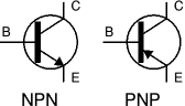
There are two types of standard transistors, NPN and PNP, with different circuit symbols. The letters refer to the layers of semiconductor material used to make the transistor. Most transistors used today are NPN because this is the easiest type to make from silicon. This page is mostly about NPN transistors and if you are new to electronics it is best to start by learning how to use these first.The leads are labelled base (B), collector (C) and emitter(E).
These terms refer to the internal operation of a transistor but they are not much help in understanding how a transistor is used, so just treat them as labels!
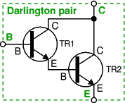
A Darlington pair is two transistors connected together to give a very high current gain.
In addition to standard (bipolar junction) transistors, there are field-effect transistors which are usually referred to as FETs. They have different circuit symbols and properties and they are not (yet) covered by this page.
Transistor currents
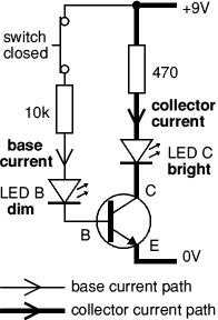 The diagram shows the two current paths through a transistor. You can build this circuit with two standard 5mm red LEDs and any general purpose low power NPN transistor (BC108, BC182 or BC548 for example).
 The small base current controls the larger collector current.
When the switch is closed a small current flows into the base (B) of the transistor. It is just enough to make LED B glow dimly. The transistor amplifies this small current to allow a larger current to flow through from its collector (C) to its emitter (E). This collector current is large enough to make LED C light brightly.
When the switch is open no base current flows, so the transistor switches off the collector current. Both LEDs are off.
A transistor amplifies current and can be used as a switch.
This arrangement where the emitter (E) is in the controlling circuit (base current) and in the controlled circuit (collector current) is called common emitter mode. It is the most widely used arrangement for transistors so it is the one to learn first.
Functional model of an NPN transistor
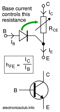 The operation of a transistor is difficult to explain and understand in terms of its internal structure. It is more helpful to use this functional model:
 - The base-emitter junction behaves like a diode.
- A base current IB flows only when the voltage VBE across the base-emitter junction is 0.7V or more.
- The small base current IB controls the large collector current Ic.
- Ic = hFE × IB (unless the transistor is full on and saturated)
hFE is the current gain (strictly the DC current gain), a typical value for hFE is 100 (it has no units because it is a ratio) - The collector-emitter resistance RCE is controlled by the base current IB:
- IB = 0 RCE = infinity transistor off
- IB small RCE reduced transistor partly on
- IB increased RCE = 0 transistor full on ('saturated')
- A resistor is often needed in series with the base connection to limit the base current IB and prevent the transistor being damaged.
- Transistors have a maximum collector current Ic rating.
- The current gain hFE can vary widely, even for transistors of the same type!
- A transistor that is full on (with RCE = 0) is said to be 'saturated'.
- When a transistor is saturated the collector-emitter voltage VCE is reduced to almost 0V.
- When a transistor is saturated the collector current Ic is determined by the supply voltage and the external resistance in the collector circuit, not by the transistor's current gain. As a result the ratio Ic/IBfor a saturated transistor is less than the current gain hFE.
- The emitter current IE = Ic + IB, but Ic is much larger than IB, so roughly IE = Ic.
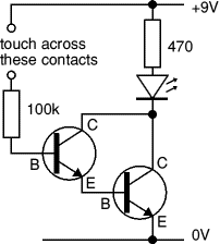
Touch switch circuit
Darlington pair
This is two transistors connected together so that the current amplified by the first is amplified further by the second transistor. The overall current gain is equal to the two individual gains multiplied together:Darlington pair current gain, hFE = hFE1 × hFE2
(hFE1 and hFE2 are the gains of the individual transistors)
This gives the Darlington pair a very high current gain, such as 10000, so that only a tiny base current is required to make the pair switch on.
A Darlington pair behaves like a single transistor with a very high current gain. It has three leads (B, C and E) which are equivalent to the leads of a standard individual transistor. To turn on there must be 0.7V across both the base-emitter junctions which are connected in series inside the Darlington pair, therefore it requires 1.4V to turn on.
Darlington pairs are available as complete packages but you can make up your own from two transistors; TR1 can be a low power type, but normally TR2 will need to be high power. The maximum collector current Ic(max) for the pair is the same as Ic(max) for TR2.
A Darlington pair is sufficiently sensitive to respond to the small current passed by your skin and it can be used to make a touch-switch as shown in the diagram. For this circuit which just lights an LED the two transistors can be any general purpose low power transistors. The 100k![]() resistor protects the transistors if the contacts are linked with a piece of wire.
resistor protects the transistors if the contacts are linked with a piece of wire.
Using a transistor as a switch
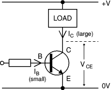 When a transistor is used as a switch it must be either OFF or fully ON. In the fully ON state the voltage VCE across the transistor is almost zero and the transistor is said to be saturated because it cannot pass any more collector current Ic. The output device switched by the transistor is usually called the 'load'.
 The power developed in a switching transistor is very small:
- In the OFF state: power = Ic × VCE, but Ic = 0, so the power is zero.
- In the full ON state: power = Ic × VCE, but VCE = 0 (almost), so the power is very small.
For information about the operation of a transistor please see the functional model above.
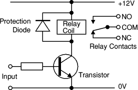
Protection diode
If the load is a motor, relay or solenoid (or any other device with a coil) a diode must be connected across the load to protect the transistor from the brief high voltage produced when the load is switched off. The diagram shows how a protection diode is connected 'backwards' across the load, in this case a relay coil.Current flowing through a coil creates a magnetic field which collapses suddenly when the current is switched off. The sudden collapse of the magnetic field induces a brief high voltage across the coil which is very likely to damage transistors and ICs. The protection diode allows the induced voltage to drive a brief current through the coil (and diode) so the magnetic field dies away quickly rather than instantly. This prevents the induced voltage becoming high enough to cause damage to transistors and ICs.
When to use a relay
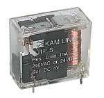
Relays
Photographs © Rapid Electronics
Transistors cannot switch AC or high voltages (such as mains electricity) and they are not usually a good choice for switching large currents (> 5A). In these cases a relay will be needed, but note that a low power transistor may still be needed to switch the current for the relay's coil!
Advantages of relays:
- Relays can switch AC and DC, transistors can only switch DC.
- Relays can switch high voltages, transistors cannot.
- Relays are a better choice for switching large currents (> 5A).
- Relays can switch many contacts at once.
- Relays are bulkier than transistors for switching small currents.
- Relays cannot switch rapidly, transistors can switch many times per second.
- Relays use more power due to the current flowing through their coil.
- Relays require more current than many ICs can provide, so a low power transistor may be needed to switch the current for the relay's coil.
Connecting a transistor to the output from an IC
Most ICs cannot supply large output currents so it may be necessary to use a transistor to switch the larger current required for output devices such as lamps, motors and relays. The 555 timer IC is unusual because it can supply a relatively large current of up to 200mA which is sufficient for some output devices such as low current lamps, buzzers and many relay coils without needing to use a transistor.A transistor can also be used to enable an IC connected to a low voltage supply (such as 5V) to switch the current for an output device with a separate higher voltage supply (such as 12V). The two power supplies must be linked, normally this is done by linking their 0V connections. In this case you should use an NPN transistor.
A resistor RB is required to limit the current flowing into the base of the transistor and prevent it being damaged. However, RB must be sufficiently low to ensure that the transistor is thoroughly saturated to prevent it overheating, this is particularly important if the transistor is switching a large current (> 100mA). A safe rule is to make the base current IB about five times larger than the value which should just saturate the transistor.
Choosing a suitable NPN transistor
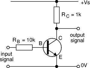
The circuit diagram shows how to connect an NPN transistor, this will switch on the load when the IC output is high. If you need the opposite action, with the load switched on when the IC output is low (0V) please see the circuit for a PNP transistor below.The procedure below explains how to choose a suitable switching transistor.
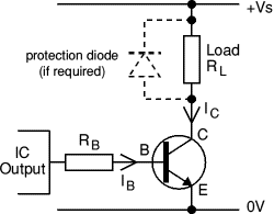
NPN transistor switch
(load is on when IC output is high)
Using units in calculations
Remember to use V, A and ![]() or
or
V, mA and k![]() . For more details
. For more details
please see the Ohm's Law page.
- The transistor's maximum collector current Ic(max) must be greater than the load current Ic.
load current Ic =
supply voltage Vsload resistance RL
- The transistor's minimum current gain hFE(min) must be at least five times the load current Ic divided by the maximum output current from the IC.
hFE(min) > 5 ×
load current Icmax. IC current
- Choose a transistor which meets these requirements and make a note of its properties: Ic(max) and hFE(min).
There is a table showing technical data for some popular transistors on the transistors page. - Calculate an approximate value for the base resistor:
RB =
Vc × hFE
where Vc = IC supply voltage
(in a simple circuit with one supply this is Vs)5 × Ic
For a simple circuit where the IC and the load share the same power supply (Vc = Vs) you may prefer to use: RB = 0.2 × RL × hFE
Then choose the nearest standard value for the base resistor.
- Finally, remember that if the load is a motor or relay coil a protection diode is required.
Example
The output from a 4000 series CMOS IC is required to operate a relay with a 100![]() coil.
coil.
The supply voltage is 6V for both the IC and load. The IC can supply a maximum current of 5mA.
- Load current = Vs/RL = 6/100 = 0.06A = 60mA, so transistor must have Ic(max) > 60mA.
- The maximum current from the IC is 5mA, so transistor must have hFE(min) > 60 (5 × 60mA/5mA).
- Choose general purpose low power transistor BC182 with Ic(max) = 100mA and hFE(min) = 100.
- RB = 0.2 × RL × hFE = 0.2 × 100 × 100 = 2000
 . so choose RB = 1k8 or 2k2.
 - The relay coil requires a protection diode.
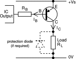
PNP transistor switch
(load is on when IC output is low)
Choosing a suitable PNP transistor
The circuit diagram shows how to connect a PNP transistor, this will switch on the load when the IC output is low (0V). If you need the opposite action, with the load switched on when the IC output is high please see the circuit for an NPN transistor above.The procedure for choosing a suitable PNP transistor is exactly the same as that for an NPN transistor described above.
Using a transistor switch with sensors
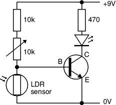
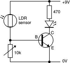
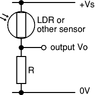
LED lights when the LDR is dark
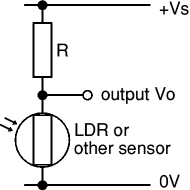
LED lights when the LDR is bright
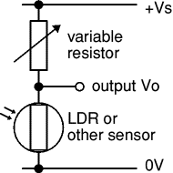
The top circuit diagram shows an LDR (light sensor) connected so that the LED lights when the LDR is in darkness. The variable resistor adjusts the brightness at which the transistor switches on and off. Any general purpose low power transistor can be used in this circuit.
The 10k![]() fixed resistor protects the transistor from excessive base current (which will destroy it) when the variable resistor is reduced to zero. To make this circuit switch at a suitable brightness you may need to experiment with different values for the fixed resistor, but it must not be less than 1k
fixed resistor protects the transistor from excessive base current (which will destroy it) when the variable resistor is reduced to zero. To make this circuit switch at a suitable brightness you may need to experiment with different values for the fixed resistor, but it must not be less than 1k![]() .
.
If the transistor is switching a load with a coil, such as a motor or relay, remember to add a protection diode across the load.
The switching action can be inverted, so the LED lights when the LDR is brightly lit, by swapping the LDR and variable resistor. In this case the fixed resistor can be omitted because the LDR resistance cannot be reduced to zero.
Note that the switching action of this circuit is not particularly good because there will be an intermediate brightness when the transistor will be partly on (not saturated). In this state the transistor is in danger of overheating unless it is switching a small current. There is no problem with the small LED current, but the larger current for a lamp, motor or relay is likely to cause overheating.
Other sensors, such as a thermistor, can be used with this circuit, but they may require a different variable resistor. You can calculate an approximate value for the variable resistor (Rv) by using a multimeter to find the minimum and maximum values of the sensor's resistance (Rmin and Rmax):
Variable resistor, Rv = square root of (Rmin × Rmax)
For example an LDR: Rmin = 100![]() , Rmax = 1M
, Rmax = 1M![]() , so Rv = square root of (100 × 1M) = 10k
, so Rv = square root of (100 × 1M) = 10k![]() .
.
You can make a much better switching circuit with sensors connected to a suitable IC (chip). The switching action will be much sharper with no partly on state.
A transistor inverter (NOT gate)
 Inverters (NOT gates) are available on logic ICs but if you only require one inverter it is usually better to use this circuit. The output signal (voltage) is the inverse of the input signal:
 - When the input is high (+Vs) the output is low (0V).
- When the input is low (0V) the output is high (+Vs).
If you are connecting the inverter to a CMOS logic IC input (very high impedance) you can increase RB to 100k![]() and RC to 10k
and RC to 10k![]() , this will reduce the current used by the inverter.
, this will reduce the current used by the inverter.


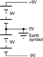
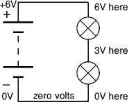 Voltage is a difference between two points, but in electronics we often refer to voltage at a point meaning the voltage difference between that point and a reference point of 0V (zero volts).