Custom Search

Tuesday, October 5, 2010

50V 2A power supply circuit design – adjustable


LM10 makes this 50V power supply a quality one. With 2 LM10 we can build a short circuit protected power supply, with adjustable output voltage and current.
The output voltage increases linear with P1 and P3 adjust the current. P2 is used for adjusting the maximum output current (2A). This 50V power supply has a minimum output voltage arround 0.4V and maximum 45V. For 50V the main transformer is 42V / 2A, C5 = 4700uF / 80V, T4 = BF257, T6, T7 = BD245B . R12 has 470Ω / 5W.
If a short circuit appears the final transistor wont burn if are cooled enough.

http://electroschematics.com

Frequency converter


This is a 35.3 to 10.7 MHz converter circuit. It converts the 35.3 MHz signal coming from a VHF/UHF tuner down to an FM tuner to decode the TV audio in FM quality. The IC being used (TBA120) is one of the most common components in radio and TV circuits. Although it was designed as an RF amplifier and FM demodulator, it can also be used for many other applications.
The circuit works according to a simple principle: a converter has always a mixer and an oscillator. The TBA120 can be used as the mixer. Its amplifier component can then be used as the oscillator by adding an LC network to it (L1/C1).
Using the values given on the diagram, the circuit oscillates at 46 MHz. This is then mixed with the input signal of 35.3 MHz rezulting to a 10.7 MHz output signal. Following this example, one can modify the circuit to convert other frequencies. The components that need to be redimensioned are the L1/C1 oscillator network and the output filter L2/C5. If the desired oscillator frequency is far below 46 MHz, the R1/C3 must also be adapted as well as the L1/C1. Both values must be increased for lower oscillator frequencies but their exact values are not very critical and can be derived experimentally.The pcb design must be very simple due to the simplicity of the circuit. However, it is highly recommended to provide lots of ground copper plating. Also, keep the copper lines short and narrow. Most specially, keep the copper lines of the decoupling capacitors to ground as short as possible.

http://electroschematics.com

PCB Placing Power and Ground Traces

 After the components are placed, the next step is to lay the power and ground traces. It is essential when working with ICs to have solid power and ground lines, using wide traces that connect to common rails for each supply. It is very important to avoid snaking or daisy chaining the power lines from part-to-part.


One common configuration is shown below. The bottom layer of the PC board includes a "filled" ground plane. Large traces feeding from a single rail are used for the positive supply.

PCB Placing Components


Generally, it is best to place parts only on the top side of the board.
When placing components, make sure that the snap-to-grid is turned on. Usually, a value of 0.050" for the snap grid is best for this job.
First place all the components that need to be in specific locations. This includes connectors, switches, LEDs, mounting holes, heat sinks or any other item that mounts to an external location.
Give careful thought when placing component to minimize trace lengths. Put parts next to each other that connect to each other. Doing a good job here will make laying the traces much easier.
Arrange ICs in only one or two orientations: up or down, and, right or left. Align each IC so that pin one is in the same place for each orientation, usually on the top or left sides.
Position polarized parts (i.e. diodes, and electrolytic caps) with the positive leads all having the same orientation. Also use a square pad to mark the positive leads of these components.
You will save a lot of time by leaving generous space between ICs for traces. Frequently the beginner runs out of room when routing traces. Leave 0.350" - 0.500" between ICs, for large ICs allow even more.
Parts not found in the component library can be made by placing a series of individual pads and then grouping them together. Place one pad for each lead of the component. It is very important to measure the pin spacing and pin diameters as accurately as possible. Typically, dial or digital calipers are used for this job.
After placing all the components, print out a copy of the layout. Place each component on top of the layout. Check to insure that you have allowed enough space for every part to rest without touching each other.

MAX2606 VHF FM Transmitter

If you want to be independent of the local radio stations for testing VHF receivers, you need a frequency-modulated oscillator that covers the range of 89.5 to 108 MHz — but building such an oscillator using discrete components is not that easy. Maxim now has available a series of five integrated oscillator building blocks in the MAX260x series which cover the frequency range between 45 and 650 MHz. The only other thing you need is a suitable external coil, dimensioned for the midrange frequency.
The MAX2606 covers the VHF band, although the frequency can only be varied by approximately ±3 MHz around the midrange frequency set by the coil L. The inductance values shown in the table can serve as starting points for further experimenting.
The SMD coils of the Stettner 5503 series are suitable for such oscillators. In Germany, they are available from Bürklin (www.buerklin.de), with values between 12 nH and 1200 nH. You can thus directly put together any desired value using two suitable coils. If you want to wind your own coils, try using 8 to 14 turns of 0.5-mm diameter silver-plated copper wire on a 5-mm mandrel. You can make fine adjustments to the inductance of the coil by slightly spreading or compressing the coil.
The circuit draws power from a 9-V battery. The BC238C stabilises the voltage to approximately 4 V. Although the MAX2606 can work with a supply voltage between +2.7 V and +5.5 V, a stabilised voltage improves the frequency stability of the free-running oscillator. The supply voltage connection Vcc (pin 5) and the TUNE voltage (pin 3) must be decoupled by 1-nF capacitors located as close as possible to the IC pins. The tuning voltage TUNE on pin 3 may lie between +0.4 V and +2.4 V. A symmetric output is provided by the OUT+ and OUT– pins. In the simplest case, the output can be used in a single-ended configuration. Pull-up resistors are connected to each of the outputs for this purpose. You can use a capacitor to tap off the radio signal from either one of these resistors. Several milliwatts of power are available. At the audio input, a signal amplitude of 10 to 20 mV is enough to generate the standard VHF frequency deviation of ±40 kHz.

http://electroschematics.com/

FM Transmitter USB

Here is a simple USB FM transmitter that could be used to play audio files from an MP3 player or computer on a standard VHF FM radio by connecting it to an USB port. The circuit use no coils that have to be wound. This USB transmitter can be used to listen to your own music throughout your home.
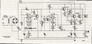
To keep the fm transmitter circuit simple as well as compact, it was decided to use a chip made by Maxim Integrated Products, the MAX2606. This IC from the MAX2605-MAX2609 series has been specifically designed for low-noise RF applications with a fixed frequency. The VCO (Voltage Controlled Oscillator) in this IC uses a Colpitts oscillator circuit. The variable-capacitance (varicap) diode and feedback capacitors for the tuning have also been integrated on this chip, so that you only need an external inductor to fix the central oscillator frequency.
It is possible to fine-tune the frequency by varying the voltage to the varicap. Not much is demanded of the inductor, a type with a relatively low Q factor (35 to 40) is sufficient according to Maxim. The supply voltage to the IC should be between 2.7 and 5.5 V, the current consumption is between 2 and 4 mA. With values like these it seemed a good idea to supply the circuit with power from a USB port. A common-mode choke is connected in series with the USB connections in order to avoid interference between the circuit and the PC supply. There is not much else to the circuit. The stereo signal connected to K1 is combined via R1 and R2 and is then passed via volume control P1 to the Tune input of IC1, where it causes the carrier wave to be frequency modulated. Filter R6/C7 is used to restrict the bandwidth of the audio signal. The setting of the frequency (across the whole VHF FM broadcast band) is done with P2, which is connected to the 5 V supply voltage.
The PCB designed uses resistors and capacitors with 0805 SMD packaging. The size of the board is only 41.2 x 17.9 mm, which is practically dongle-sized. For the aerial an almost straight copper track has been placed at the edge of the board. In practice we achieved a range of about 6 metres (18 feet) with this fm transmitter usb. There is also room for a 5-way SIL header on the board. Here we find the inputs to the 3.5 mm jack plug, the input to P1 and the supply voltage. The latter permits the circuit to be powered independently from the mains supply, via for example three AA batteries or a Lithium button cell. Inductor L1 in the prototype is a type made by Murata that has a fairly high Q factor: minimum 60 at 100 MHz. Take care when you solder filter choke L2, since the connections on both sides are very close together. The supply voltage is connected to this, so make sure that you don’t short out the USB supply! Use a resistance meter to check that there is no short between the two supply connectors before connecting the circuit to a USB port on a computer or to the batteries.
P1 has the opposite effect to what you would expect (clockwise reduces the volume), because this made the board layout much easier. The deviation and audio bandwidth varies with the setting of P1. The maximum sensitivity of the audio input is fairly large. With P1 set to its maximum level, a stereo input of 10 mVrms is sufficient for the sound on the radio to remain clear. This also depends on the setting of the VCO. With a higher tuning voltage the input signal may be almost twice as large (see VCO tuning curve in the data sheet). Above that level some audible distortion becomes apparent. If the attenuation can’t be easily set by P1, you can increase the values of R1 and R2 without any problems.
Measurements with an RF analyzer showed that the third harmonic had a strong presence in the transmitted spectrum (about 10 dB below the fundamental frequency). This should really have been much lower. With a low-impedance source connected to both inputs the bandwidth varies from 13.1 kHz (P1 at maximum) to 57 kHz (with the wiper of P1 set to 1/10).
In this usb fm transmitter circuit the pre-emphasis of the input is missing. Radios in Europe have a built-in de-emphasis network of 50 μs (75 μs in the US). The sound from the radio will therefore sound noticeably muffled. To correct this, and also to stop a stereo receiver from mistakenly reacting to a 19 kHz component in the audio signal, an enhancement circuit Is published elsewhere in this issue (Pre-emphasis for FM Transmitter, also with a PCB).

usb transmitter components list

MP3 FM Transmitter Parts List
Resistors (all SMD 0805)
R1,R2 = 22kΩ
R3 = 4kΩ7
R4,R5 = 1kΩ
R6 = 270Ω
P1 = 10kΩ preset, SMD (TS53YJ103MR10 Vishay Sfernice, Farnell # 1557933)
P2 = 100kΩ preset, SMD(TS53YJ104MR10 Vishay Sfernice, Farnell # 1557934)
Capacitors (all SMD 0805)
C1,C2,C5 = 4μF7 10V
C3,C8 = 100nF
C4,C7 = 2nF2
C6 = 470nF
Inductors
L1 = 390nF, SMD 1206 (LQH31HNR39K03L Murata, Farnell # 1515418)
L2 = 2200Ω @ 100MHz, SMD, common-mode choke, 1206 type(DLW31SN222SQ2L Murata, Farnell #1515599)
Semiconductors
IC1 = MAX2606EUT+, SMD SOT23-6 (Maxim Integrated Products)
Miscellaneous
K1 = 3.5mm stereo audio jack SMD (SJ1-3513-SMT
CUI Inc, DIGI-Key # CP1-3513SJCT-ND)
K2 = 5-pin header (only required in combination with 090305-I pre-emphasis circuit)
K3 = USB connector type A, SMD (2410 07 Lumberg, Farnell # 1308875)

source:http://www.fmtvguide.blogspot.com

1W fm transmitter

A very good 1 watt fm transmitter circuit, very easy to build circuit. It has 4 transistors, one is a very stable oscillator, followed by a buffer stage to prevent frequency variation when you adjust the transmitter. Next is a resonance stage and the final stage built with a minimum 1W transistor which must have a heatsink. You must use a LM7805 stabilizer for the oscillator diodes and one LM7809 for powering up the T1 oscillator stage. This will give you a very stable transmitter frequency.
First build the oscillator stage and the buffer, power it up and trim the 10k linear potentiometer untill you can here a blank signal on your receiver. If you put a small piece of wire on the T2 emitter you can see that the cover range of the 2 stage transmitter is about 3 meter.
After you are sure that your oscillator+buffer stage are working properly, remove the power supply and continue building the T3 resonance stage. Connect the power supply and if you adjust the trimmer (variable capacitor) from T3 collector you can see how the fm transmitter power can be varied. This stage is very important for proper functionality of the entire 1 watt fm transmitter. You must adjust the trimmer for maximum power.

1 Watt fm transmitter adjustment

The final stage of the 1W fm transmitter is built with 2N4427 (recommended) or the transistors from the list. If you can’t find any, use a BD139 transistor but only for frequencies lower than 90 MHz. The output power will be lower but you get the idea. If you decide to use 2N2219 transistor for the final stage of the transmitter you must know that the output rf power will be 0.4W.
Adjust the last 2 trimmers for maximum output power in the antenna. Initially use 2 x 100 Ω 0.5W resistors in parallel at the RF output. Then connect this rf probe to the output and adjust all the 3 trimmers starting from T3 to output. You must adjust it to obtain the maximum multimeter indication. Then power it off, connect the antenna and make the final adjustments for maximum broadcasting coverage distance.
The oscillator and buffer stage must be enclosed in a 1 mm copper case, then do the same with the T3 and T4 stages.
Use a 12Vdc power supply to power up this fm broadcast circuit. T4 will have a current consumption of around 150 mA at full power output adjustments. The total current consumption of the entire 1 watt transmitter will be around 500 mA.

http://electroschematics.com

FM Wireless Microphone


This simple FM wireless microphone transmitter can transmit speech over a short range. It can be used as a simple cordless microphone. The circuit uses two integrated circuits from Maxim. IC1 a MAX4467, is an amplifier raising the microphone signal to a level suitable for frequency modulation (FM). IC2 is a voltage-controlled oscillator (VCO) with integrated varactor (a.k.a. varicap diode). It is this small that can be integrated in a wireless handheld microphone.
The wireless microphone nominal frequency of oscillation is set by inductor L1. The inductor value 390 nH provides an oscillation frequency of about 100 MHz. For best performance, L1 should be a high-Q component. L1 may consist of 4 turns of silver-plated wire wound around a 10-mm drill bit, and stretched to a length of about 1.5 cm. The wire diameter can be anything between 26 SWG (0.5 mm) and 20 SWG (1 mm). No core is used.
The MAX4467 is a micropower opamp for low voltage operation and providing 200-kHz gain bandwidth at a supply current of just 24 μA. When used with an electret microphone, some form of DC bias for the microphone capsule is necessary. The MAX4467 has the ability to turn off the bias to the microphone when the device is in shutdown mode. This can save several hundred microamps of supply current, which can be significant in low power applications particularly for battery powered applications like cordless microphones. The MICBias pin provides a switched version of Vcc to the bias components.

http://electroschematics.com/

FM Radio Transmitter

A simple fm radio transmitter circuit which covers frequencies from 88 to 108 MHz. It is built with 3 transistors: BC109, BFR91A and BFR96S. It is quite stable and the output power is around 200 mW.
The first stage in a mic amplifier but if you connect this radio transmitter directly to an audio source you can remove this stage and connect the audio signal to R5.U1, 1PH51C can be replaced with LM7805. You must use a stabilized power source for oscillator stage to prevent frequency variation. You can remove C7 and use a linear potentiometer insted of R6 with the median connector to C4, one pin to ground and the other one to +. You may replace BB109 varicap diode with BB139.

All coils must be perpendicular one to the other, especially L2 and L3. The oscillator stage must be encased with a copper 1mm foil. If you use an external antenna, like this fm dipole antenna connect it with a good coaxial cable because the power is low and you want to use most of it. If you don’t want to loose the rf power connect the radio transmitter close to the antenna (2 meter coaxial cable) and use a longer cable for the audio signal (coaxial). If you connect the antenna as I told you before you can cover a 300 meter in diameter area.

http://electroschematics.com/2498/radio-transmitter-circuit/

Small FM Receiver

This is the most simple fm radio receiver with good performances that works great even if the sensitivity is not too high. The working principle of this fm receiver may seem a little unusual. It is made of an oscillator (T2 and T3) that is synchronized with the received frequency of T1. This transistor works as a broadband preamplifier in VHF range.The oscillator is adjusted between 87 … 108 MHz with C5. Because of the synchronization, the oscillator output will have the same frequency deviation as the received signal from the fm antenna. This deviations are caused by the broadcasted audio informations. The frequency modulated signal show up on P1 + R5. Low pass filter R6/C6 extracts the audio signal and then is amplifier by T4 … T6 and transmitted at the output through C9 capacitor.The coil details are presented in the fm receiver circuit diagram. The radio receiver is adjusted on different stations with the help of C5. P1 potentiometer is adjusted untill the best reception is obtained. If we attach an audio amplifier and a speaker then this fm receiver can be made very compact as a pocket radio.

http://electroschematics.com/

FM modulator

The FM modulator circuit (frequency modulation) is built with a Motorola MC1648P oscillator. Two varactors, Motorola MV-209 are used to frequency modulate the oscillator. The 5000 Ω potentiometer is used to bias the varactors for the best linearity. The output frequency of approximately 100 MHz can be adjusted by changing the value of the inductor. The output frequency can vary as much 10 MHz on each side. The output level of the modulator is -5 dBm. In this fm modulator prototype the varactor bias was 7.5V for the best linearity but this could be different with other varactors.


http://electroschematics.com/889/fm-modulator/