Custom Search

Friday, October 29, 2010

DC Power supply adjust voltage regulator 1.5 Volt - 15Volt 3Amp


I wants DC Power supply adjust voltage regulator 1.5 Volt - 15Volt, and give current about 3 Amp for in the work experiences all electronics. As seek many the circuit , meet that this circuit easily , use integrated number circuit LM1084 for control voltage model regulator adjustable voltage 1.5V - 15V. With fining decorates VR1. And should feedInput AC 18V 3A low like besides should hold let off the heat gives the integrated circuit LM1084 with. For the detail , see in the circuit.


http://www.circuitpowersupply.com/circuitblog/dc-power-supply-adjust-voltage-regulator-15-volt-15volt-3amp/

24V Variable DC Power Supply


A Variable DC Power Supply is one of the most useful tools on the electronics hobbyist’s workbench. This circuit is not an absolute novelty, but it is simple, reliable, “rugged” and short-proof, featuring variable voltage up to 24V and variable current limiting up to 2A.


Well suited to supply the circuits shown in this website. You can adapt it to your own requirements as explained in the notes below.
Link :

3-30V 2.5A Stabilized power supply


This is a very useful project for anyone working in electronics. It is a versatile power supply that will solve most of the supply problems arising in the everyday work of any electronics work shop. It covers a wide range of voltages being continuously variable from 30 V down to 3 V.

The output current is 2.5 A maximum, more than enough for most applications. The circuit is completely stabilised even at the extremes of its output range and is fully protected against short-circuits and overloading.
Link

10A Variable Regulator power supply with LM350


This be Variable Regulator power supply Circuit. That be High Current Source 10amp. By use the integrated circuit LM350. Which usual it controls Voltage output get 1.2V to 25V and give current about 3Amp.

But when bring parallel 3 pcs. Can give current output be 10Amp max for this circuit. It can adjustable voltage output get 4.5V to 25V at 10Amp. Other detail please see in the website Link.

Monday, October 25, 2010

L200 DC Variable power 3-15volt at 2Amp


For the work experiences general that want power supply LAB. I thinks L200 DC Variable power Circuit. May like you , because of give Volt range about 3V-15V and Current 2A normal. When , you see the circuit. May search eyes and the integrated circuit that use be number L200 although old already.


L200 DC Variable power 3-15volt at 2Amp
But still be usable well the interesting. This important circuit that should use Transformer that be appropriate be 12V sizes and should use 2A more than because get current that straight follow want certainly give testimony grandmother horn forget to stick let off the heat gives with, IC L200 with appropriately. The detail is other see in the circuit and from original website
 
http://www.mitedu.freeserve.co.uk/Circuits/Power/l200var.html

2N3055 variable supply 0-25V


One your friend beg for model the circuit about variable supply range 0-25V. I tries to search see meet voltage regulators circuits. The this be the circuit that use the transistor 2N3055 numbers are important equipment. Which be the equipment that seek good easy. fine P1 control current output the topmost.And fine P2 control Voltage range 0-25V.


2N3055 variable supply 0-25V
The detail is other invite read in original website http://www.redcircuits.com//Page36.htm

Variable Regulater Switching LAB Supply 50V 5A by TL494


Somsak is person see the website of me take an interest try build Variable Regulater Switching LAB Supply. By fine decorate voltage output get 0-50V and fine current get 5A. I then choose this circuit , which use IC TL494 be pillar equipment (Switchmode Pulse Width Modulation Control Circuit).


Variable Regulater Switching LAB Supply 50V 5A by TL494
And use pretty litter transistor number MJ15004 then give current get enough tall. But should choose pot size modifies about 5A go up with. When see the circuit has already may inappropriate with a novice. Because use many equipments then the gift uses the tie perhaps specially with , be lucky sir.
 
http://www.circuitpowersupply.com/circuitblog/variable-regulater-switching-lab-supply-50v-5a-by-tl494/

Simple DC voltage regulated 0-30V 3A


If you are looking for DC Voltage Reulator be simple. That can give Current tall about 3A and fine voltage get from 0-30V. As a result please consider this circuit before, it is easy. Because of have no the integrated circuit. Use the transistor is a principle especially the number MJ3001.


Simple DC voltage regulated 0-30V 3A
Usability just fine VR1 for control Volt output and choose the value Current get with S1. The detail is other see in the circuit help understand go up sir.

http://www.circuitpowersupply.com/circuitblog/simple-dc-voltage-regulated-0-30v-3a/

High Current Regulated Supply By LM317 and 2N3055×2


The high current regulator below uses an additional winding or a separate transformer to supply power for the LM317 regulator so that the pass transistors can operate closer to saturation and improve efficiency. For good efficiency the voltage at the collectors of the two parallel 2N3055 pass transistors should be close to the output voltage.
High Current Regulated Supply By LM317 and 2N3055×2
The LM317 requires a couple extra volts on the input side, plus the emitter/base drop of the 3055s, plus whatever is lost across the (0.1 ohm) equalizing resistors (1volt at 10 amps), so a separate transformer and rectifier/filter circuit is used that is a few volts higher than the output voltage. The LM317 will provide over 1 amp of current to drive the bases of the pass transistors and assumming a gain of 10 the combination should deliver 15 amps or more.
By Bill Bowden
Source :: http://ourworld.compuserve.com/homepages/Bill_Bowden/page12.htm

DC Voltage Regulator dual Power Supply +5V to +25V, -5V to -25V 1A with LM7805 LM7905


When you want Dual power supply Variable Regulator be simple. I begs for to advise this circuit, because use the integrated circuit LM7805 and LM7905. Make have Voltage +5V to +25V and -5V to -25V unless. Still pay current get about 1A enough with general usability.


DC Voltage Regulator dual Power Supply +5V to +25V, -5V to -25V 1A with LM7805 LM7905
The important factor is you should use Transformer at enough size doesn’t lower 2A and IC all stick let off the heat with. The detail is other see in circuit picture better sir.

http://www.circuitpowersupply.com/circuitblog/dc-voltage-regulator-dual-power-supply-5v-to-25v-5v-to-25v-1a-with-lm7805-lm7905/

2V to 25V Power Supply Schematic


This project uses a LM338 adjustable 3 terminal regulator to supply a current of up to 5A over a variable output voltage of 2V to 25V DC. It will come in handy to power up many electronic circuits when you are assembling or building any electronic devices. The schematic and parts list are designed for a power supply input of 240VAC. Change the ratings of the components if 110VAC power supply input is required.


As shown in the figure above, the mains input is applied to the circuit through fuse F1. The fuse will blow if a current greater than 8A is applied to the system. Varistor V1 is used to clamp down any surge of voltage from the mains to protect the components from breakdown. Transformer T1 is used to step down the incoming voltage to 24V AC where it is rectified by the four diodes D1, D2, D3 and D4. Electrolytic capacitor E1 is used to smoothen the ripple of the rectified DC voltage.

Diodes D5 and D6 are used as a protection devices to prevent capacitors E2 and E3 from discharging through low current points into the regulator. Capacitor C1 is used to bypass high frequency component from the circuit. Ensure that a large heat sinkis mounted to LM338 to transfer the heat generated to the atmosphere.

Parts List


http://www.electronics-project-design.com/PowerSupplySchematic.html

Simple DC Motor Driver


This simple DC motor driver circuit uses a 741 operational amplifier operating as a voltage follower where its non inverting input is connected to the speed and rotation direction of a potentiometer VR1. When VR1 is at mid position, the op-amp output is near zero and both Q1 and Q2 is OFF.

When VR1 is turned towards the positive supply side, the output will go positive voltage and Q1 will supply the current to the motor and Q2 will be OFF. When VR1 is turned to the negative supply side, the op-amp output switches to the negative voltage and Q1 will turn OFF and Q2 ON which reverses the rotation of the motor's direction.

As the potentiometer VR1 is moved toward either end, the speed increases in whichever direction it is turning.

The TIP3055 Q1 NPN power transistor has a collector current specs of 15A and VCE0 of 60V DC.

The MJE34 Q2 PNP power transistor has a collector current specs of 10A and VCE0 of 40V DC.

Parts List


Source : Extracted from Popular Electronics Nov 1997, By Charles D. Rakes

DC Servo Motor Basics


A Servo Motor is a small device that has an output shaft which can be positioned to specific angular positions by sending the servo a Pulse Coded Modulation signal. As the coded signal changes, the angular position of the shaft changes. DC servo motors are used in radio controlled airplanes, radio controlled cars, robots and a host of other applications that one can think of. A picture of a servo motor is as shown below.

Though the servo is small in size, it has a printed circuit board with control circuit built in and a standard servo manufactured by Futaba is model S3003. The power consumed is proportional to the mechanical load, thus saving energy when it is used in a varying type of load. The servo motor consist of a motor, gears and its casing. Three wires are used to interface to other control circuitry which are +5V DC, Ground and Control Signal.

It is using a control called proportional control of which the amount of power applied to the motor is proportional to the distance it needs to travel. This means that if the shaft needs to turn a large distance, the motor will run at higher speed. Usually a servo is used to control an angular motion of between 0 and 180 degrees.

The servo expects to see a pulse every 20 milliseconds (.02 seconds). The length of the pulse will determine how far the motor turns. A 1.5 millisecond pulse, for example, will make the motor turn to the 90 degree position (often called the neutral position). If the pulse is shorter than 1.5 ms, then the motor will turn the shaft to closer to 0 degress. If the pulse is longer than 1.5ms, the shaft turns closer to 180 degress.

DC Servo Motor Driver Circuit Description

The input signals are between 0 - 5V delivered by connecting up the 10K potentiometers as voltage dividers. The Microchip PIC 16C71 has an AD converter that changes the voltage signal into the Pulse Code Modulation system used by the servo motors. This signal is a 5V pulse between 1 and 2 msec long repeated 50 times per second. The width of the pulse determines the position of the server. Most servos will move to the center of their travel when they receive a 1.5msec pulse. One extreme of motion generally equates to a pulse width of 1.0msec; the other extreme to 2.0msec with a smooth variation throughout the range, and neutral at 1.5msec.

It will be a good experience to experiment the control of servo motors in this project by doing your own software programming using PIC 16C71 microcontroller.


http://www.electronics-project-design.com/DCservoMotor.html

Sunday, October 24, 2010

Controlling the speed of 3 phase induction motors

The speed of a normal 3-phase induction motor is a function of the frequency of the supply voltage. Changing the speed of such a motor hence requires building a 3-phase power frequency convertor. The driver can be realised using power mosfets (or IGTB's) capable of handling high voltages and fast switching speeds. The generated frequency can be programmed in a small PIC controller and even in a fast Basic Stamp.

Note that at lower than normal frequencies, the voltage should be decreased proportionally. If you forget this, the motor may overheat and eventually even burn out. (See note at the bottom of this paragraph). The circuits shown here serve mere educational purposes (although they do work!) and are not always the most suitable nor safest sollution.

For the bipolar drive circuit shown below, the motor should be delta-connected.

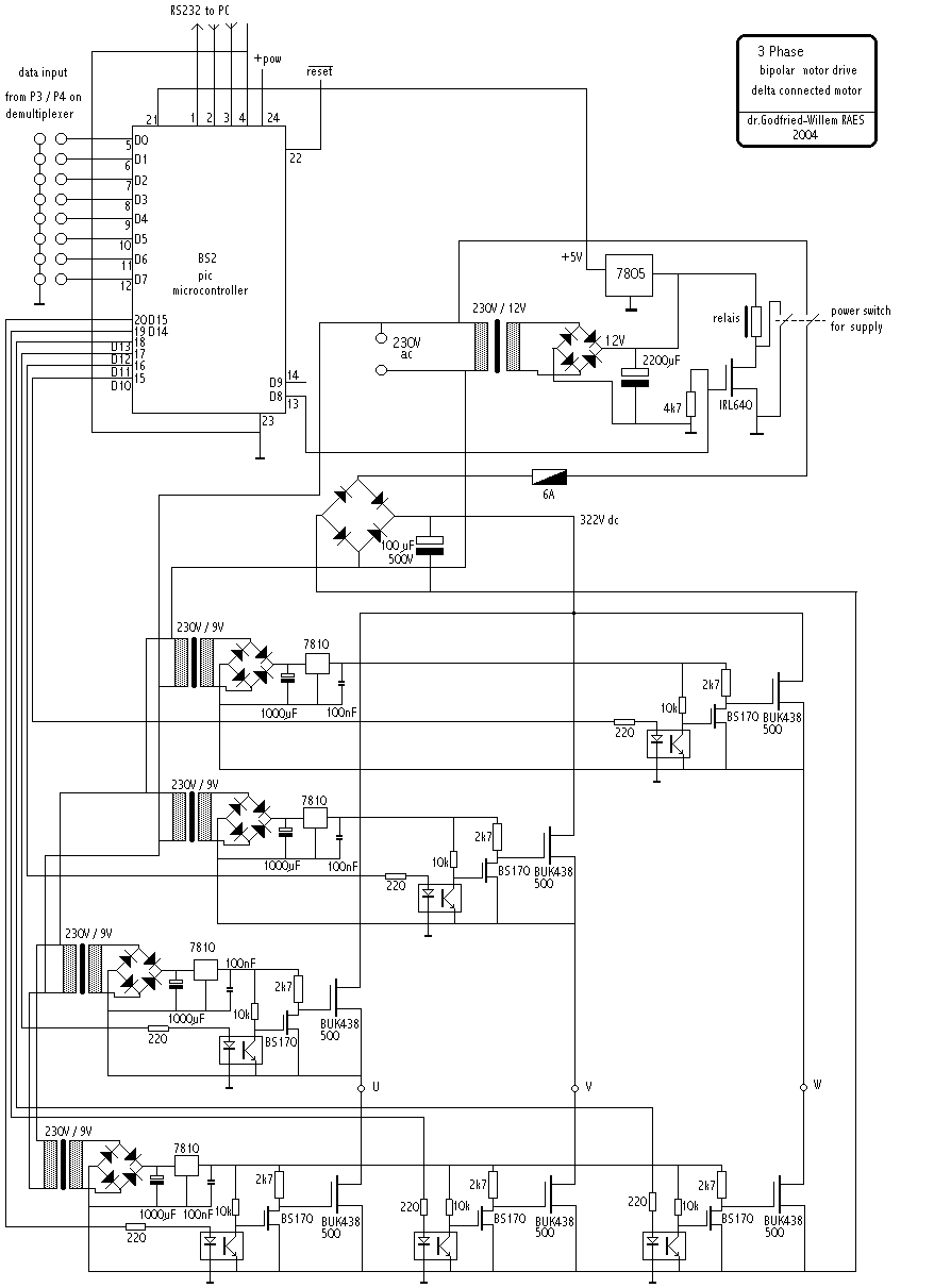
The optocouplers used can be either TIL111 or CNY17-2. Do not try to save on the transformers: these are very small and cheap types (2VA is enough) and the floating way they are connected here (no grounded negative poles!) is essential to this design. Be carefull when playing around with this kind of circuitry, since there are high voltages everywhere. The digital input and the microcontroller are completely and optically isolated from the power circuitry.

The bit-pattern to be programmed in the controller software could look like:

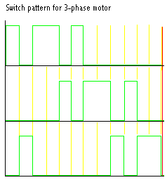
Note the 120 degree phase shift. The pattern was designed to generate a lot of thirth harmonic distortion on the resulting wave, thus increasing the RMS voltage over the motor windings.

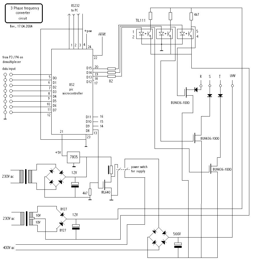
If you want the motor to be Y-connected, the problem will be that you need a much higher voltage to work from. Using a 3-phase rectifier bridge, you can of course use rectified 3-phase mains current, but that presupposes its availability. Ass an alternative an insulation transformer 230V/ 400V can be used. However, at the end this will tend to be more expensive than the circuit given above. The circuit below however will become a lot simpler, since we do not require 6 mosfets and no floating powers supplies:

Applications:

  • changing/ adjusting the wind pressure in windblown organs.
  • Motor controllers for lathes, large saws etc...
  • 3-phase current generator
  • Brushless DC motor drives

NOTE:

If you are in need of a controller for a 3-phase motor, you should always consider using one of the many modules the industry offers these days. Factories such as Lust gmbh, Siemens (Micromaster 410), Toshiba, Hitachi... all have controll modules in their catalogues. Controlling the speed of the motor using such a standard solution can be done by sending an analog voltage (0-10V most of the time) to the appropriate input, or, on some models, by sending RS232 commands to their port. The advantage of these modules is, amongst other things, that they serve as a motor protector at the same time. Also, it might at the end be cheaper than building the circuits shown above yourself.


http://www.logosfoundation.org/kursus/2113.html

6-transistor H-bridge


This is the six transistor "Tilden style" H-bridge; while not as old as the original "basic H-bridge," this goes "way back," and is the basis for many BEAM driver circuits

  • Up to 800 mA capacity (using PN2222 and PN2907 transistors)
  • 30 connections per bridge (so, 30 holes if you make a PCB)
  • Not "smoke-proof" (i.e., it can't handle drive voltage in both directions at once)


You can read the original Tilden article (complete with ASCII art) here.

This circuit comes in two flavors -- one triggers on positive input (non-inverting), the other triggers on negative input (inverting).

Freeforming Courtesy of Bruce Robinson, here are diagrams for free-forming both the inverting and non-inverting flavors of this circuit (note that these are drawn "dead bug" style, i.e., with leads "up"):

ImageImage

Bruce Robinson explains:

I did a couple of revised drawings for Ian quite a while back, so he could put them up at beam-online. Unfortunately, they didn't get posted in the midst of the many revisions he was making.

Attached (begging Ian's indulgence), are the two versions of the circuit, one which turns on with a Positive input, the other (for quadcores) with a Negative input.

Ian shows 100k input resistors. I've been using 47k resistors successfully. Tilden's article recommends nothing lower than 50k (I assumed 47k was close enough) and up to 20 Meg or so.

I've also noticed a slight drop in speed when I use these bridges, but only about 10% or so.

http://library.solarbotics.net/circuits/driver_tilden.html

4-transistor H-bridge

Steve Bolt came up with an interesting 4-transistor H-bridge variant; this is cheap and easy to build, and best of all is "smokeless" (i.e., no combination of inputs can cause the bridge to self-destruct). Here's Steve's diagram:

Image

You should bear the following things in mind with this design:

  • 2N2905 and 2N2219 transistors are no longer being produced; I use 2N2907 and 2N2222 transistors in this circuit, with good results.
  • You absolutely must use one bias resistor per transistor; I attempted to simplify the circuit by connecting the respective transistors' bases (so each pair of transistors could "share" a resistor) -- this made for a circuit that was simpler, much easier to freeform, and completely non-functional.
  • This efficiency of this design is driven by 2 things -- the efficiency of the motor it's driving, and the size of the bias resistors. Just to make life interesting, these things are interrelated (more on this later).
  • This bridge is "smokeable" -- but only if power is supplied to the bridge while the control inputs are allowed to "float" (easy thing to avoid in yourcircuit design).
  • When I first started tinkering with this circuit, I made the assumption that the inverters pictured in Steve's diagram were not intrinsic parts of the bridge, but instead were examples of the outputs coming from the "driving" circuit. This is very, very wrong. If you don't include inverters (or, at least buffers) on the control inputs, you now have to take great care to avoid having the bridge influence the circuit that's driving it.

Since your circuit may or may not (and most likely, won't) have spare buffers / inverters available for use on the H-bridge control inputs, I've done some experimenting on the bridge circuit sans inverters -- let's call this variant "Bolt light."

Freeforming

If you want to build a "freeform" version of the "Bolt light" circuit, here's a very compact layout (note that this diagram shows the transistors in "dead-bug" fashion, i.e., with the chips "down," and their legs pointing up towards you).

I've found it's easiest to solder the outside (motor lead) connections first, then the inside (Vcc / ground) connections, then the middle (resistor) connections. Note that two resistor leads "bridge over" the top of the transistor packages (these hidden leads are shown as dashed lines).


http://library.solarbotics.net/circuits/driver_4varHbridge.html

Thursday, October 21, 2010

Pump Controller For Solar Hot Water System

This circuit optimises the operation of a solar hot water system. When the water in the solar collector is hotter than the storage tank, the pump runs. The circuit comprises two LM335Z temperature sensors, a comparator and Mosfet. Sensor 1 connects to the solar collector panel while Sensor 2 connects to the hot water panel. Each sensor includes a trimpot to allow adjustment of the output level. In practice, VR1 and VR2 are adjusted so that both Sensor 1 and Sensor 2 have the same output voltage when they are at the same temperature. The Sensor outputs are monitored using comparator IC1.
When Sensor 1 produces a higher voltage than Sensor 2, which means that sensor 1 is at a higher temperature, pin 1 of IC1 goes high and drives the gate of Mosfet Q1. This in turn drives the pump motor. IC1 includes hysteresis so that the output does not oscillate when both sensors are producing a similar voltage. Hysteresis comprises the 1MO feedback resistor between output pin 1 and non-inverting input pin 3 and the input 1kO resistor. This provides a nominal 12mV hysteresis so that voltage at Sensor 1 or Sensor 2 must differ by 12mV for changes in the comparator output to occur.
Circuit diagram:

Pump controller for solar hot water system circuit schematic

Since the outputs of Sensor 1 and Sensor 2 change by about 10mV/°C, we could say that there is a degree of hysteresis in the comparator. Note that IC1 is a dual comparator with the second unit unused. Its inputs are tied to ground and pin 2 of IC1 respectively. This sets the pin 7 output high. Since the output is an open collector, it will be at a high impedance. Mosfet Q1 is rated at 60A and 60V and is suitable for driving inductive loads due to its avalanche suppression capability. This clamps any inductively induced voltages exceeding the voltage rating of the Mosfet.
The sensors are adjusted initially with both measuring the same temperature. This can be done at room temperature; adjust the trimpots so that the voltage between ground and the positive terminal reads the same for both sensors. If you wish, the sensors can be set to 10mV/°C change with the output referred to the Kelvin scale which is 273K at 0°C. So at 25°C, the sensor output should be set to (273 + 25 = 298) x 10mV or 2.98V.
Note:
The sensors will produce incorrect outputs if their leads are exposed to moisture and they should be protected with some neutral cure silicone sealant. The sensors can be mounted by clamping them directly to the outside surface of the solar collector and on an uninsulated section of the storage tank. The thermostat housing is usually a good position on the storage tank.

Author: John Clarke - Copyright: Silicon Chip Electronics

Bipolar Stepper Motor Control

First, we want to explain how such a controller works and what’s involved. A bipolar motor has two windings, and thus four leads. Each winding can carry a positive current, a negative current or no current. This is indicated in Table 1by a ‘+’, a ‘–‘ or a blank. A binary counter (IC1) receives clock pulses, in response to which it counts up or down (corresponding to the motor turning to the left or the right). The counter increments on the positive edge of the pulse applied to the clock input if the up/down input is at the supply level, and it decrements if the up/down input is at earth level.
Bipolar Stepper Motor Control circuit diagramThe state of the counter is decoded to produce the conditions listed in Table 2. Since it must be possible to reverse the direction of the current in the winding, each winding must be wired into a bridge circuit. This means that four transistors must be driven for each winding. Only diagonally opposed transistors may be switched on at any given time, since otherwise short circuits would occur. At first glance, Table 2 appears incorrect, since there seem to always be four active intervals. However, you should consider that a current flows only when a and c are both active. The proper signals are generated by the logic circuitry, and each winding can be driven by a bridge circuit consisting of four BC517 transistors.

table 1Two bridge circuits are needed, one for each winding. The disadvantage of this arrangement is that there is a large voltage drop across the upper transistors in particular (which are Darlingtons in this case). This means that there is not much voltage left for the winding, especially with a 5-V supply. It is thus better to use a different type of bridge circuit, with PNP transistors in the upper arms. This of course means that the drive signals for the upper transistors must be reversed. We thus need an inverted signal in place of 1a. Fortunately, this is available in the form of 1d.
table 2The same situation applies to 1b (1c), 2a (2d) and 2b (2c). In this case, IC4 is not necessary. Stepper motors are often made to work with 12V. The logic ICs can handle voltages up to 15 to 18 V, so that using a supply voltage of 12 V or a bit higher will not cause any problems. With a supply voltage at this level, the losses in the bridge circuits are also not as significant. However, you should increase the resistor values (to 22 kΩ, for example). You should preferably use the same power supply for the motor and the controller logic. This is because all branches of the bridge circuit will conduct at the same time in the absence of control signals, which yields short-circuits.


http://www.extremecircuits.net/2010/07/bipolar-stepper-motor-control.html

Baud Rate Generator

In this article, an RC oscillator is used as a baud rate generator. If you can calibrate the frequency of such a circuit sufficiently accurately (within a few percent) using a frequency meter, it will work very well. However, it may well drift a bit after some time, and then…. Consequently, here we present a small crystal-controlled oscillator. If you start with a crystal frequency of 2.45765 MHz and divide it by multiples of 2, you can very nicely obtain the well-known baud rates of 9600, 4800, 2400, 600, 300, 150 and 75. If you look closely at this series, you will see that 1200 baud is missing, since divider in the 4060 has no Q10 output!

Baud Rate Generator circuit diagram

If you do not need 1200 baud, this is not a problem. However, seeing that 1200 baud is used in practice more often than 600 baud, we have put a divide-by-two stage in the circuit after the 4060, in the form of a 74HC74 flip-flop. This yields a similar series of baud rates, in which 600 baud is missing. The trimmer is for the calibration purists; a 33 pF capacitor will usually provide sufficient accuracy. The current consumption of this circuit is very low (around 1mA), thanks to the use of CMOS components.


http://www.extremecircuits.net/2010/07/baud-rate-generator.html

Tuesday, October 19, 2010

Electric Guitar Preamplifier

Here is the circuit diagram of a guitar preamplifier that would accept any standard guitar pickup. It is also versatile in that it has two signal outputs. A typical example of using a pick-up attached to a guitar headstock is shown inFig. 1. The pickup device has a transducer on one end and a jack on the other end. The jack can be plugged into a preamplifier circuit and then to a power amplifier system. The pickup device captures mechanical vibrations, usually from stringed instruments such as guitar or violin, and converts them into an electrical signal, which can then be amplified by an audio amplifier. It is most often mounted on the body of the instrument, but can also be attached to the bridge, neck, pick-guard or headstock.

Photo Of Electric Guitar PreamplifierThe first part of this preamplifier circuit shown in Fig. 2 is a single-transistor common-emitter amplifier with degenerative feedback in the emitter and a boot-strapped bias divider to secure optimal input impedance. With the component values shown here, the input impedance is above 50 kilo-ohms and the peak output voltage is about 2V RMS. Master-level-control potentiometer VR1 should be adjusted for minimal distortion. The input from guitar pickup is fed to this preamplifier at J1 terminal. The signal is buffered and processed by the op-amp circuit wired around IC TL071 (IC1). Set the gain using preset VR2. The circuit has a master and a slave control. RCA socket J2 is the master signal output socket and socket J3 is the slave.

Electric Guitar Preamplifier Circuit DiagramIt is much better to take the signal from J2 as the input to the power amplifier system or sound mixer. Output signals from J3 can be used to drive a standard headphone amplifier. Using potentiometer VR3, set the slave output signal level at J3. House the circuit in a metallic case. VR1 and VR3 should preferably be the types with metal enclosures. To prevent hum, ground the case and the enclosures. A well-regulated 9V DC power supply is crucial for this circuit. However, a standard 9V alkaline manganese battery can also be used to power the circuit. Switch S1 is a power on/off switch.

Source:EFY Mag

High-Intensity, Energy-Efficient LED Light

Here is a rechargeable LED lamp that gives you bright light for a long duration of time as it consumes little power. The circuit presented here is compact, automatic, reliable, low-cost and easy to assemble. The circuit comprises power supply, battery charging and switching sections. The power supply section takes power from 230V AC mains supply without using a transformer.

High-Intensity, Energy-Efficient LED Light Circuit Diagram

Capacitor C1 is used as an AC voltage dropper a well-known transformer-less solution. This helps to make the circuit compact without generating heat, as capacitor C1 dissipates negligible power. Capacitor C1 also protects against fluctuations in mains.

Current required for the battery charging circuit is provided by capacitor C1. Capacitor C1 discharges through resistor R1 when the circuit is disconnected from the mains voltage. This helps to prevent a fatal shock due to any voltage remaining in the input terminals. Capacitor C1 must be rated at least 440V AC, with mains application class X2. The AC mains voltage after capacitor C1 is given to bridge rectifier diodes D1 through D4 to convert alternating current into direct current and filtered by capacitor C2. The voltage from point B+ is given to positive terminal of the battery (BATT), anodes of LEDs (LED2 through LED21) and transistor base-bias resistor R3 through slide switch S1.

The circuit is operated in three modes (AC/charge, off and batt) by using three-position switch S1. When switch S1 is in middle position, the circuit is off. When S1 is towards right, white LEDs glow by drawing power from 4V battery. When S1 is towards left, the circuit connects to AC mains and battery starts charging. The presence of AC mains voltage and battery charging is indicated by LED1. White LEDs remain off if AC mains supply is available and glow in the absence of AC mains. When switch S1 is towards left position and AC mains is available, the battery charges through diode D6 and the white LEDs don’t glow. The negative DC path through diode D5 makes the transistor cut-off, preventing the battery current from LEDs to the negative terminal through the transistor.

Thus the white LEDs don’t glow. On the other hand, if AC mains is not available, charging stops and the base of transistor SS8050 gets positive voltage from the battery through slide switch S1 and resistor R3. The transistor conducts and the current flows from the battery’s positive terminal to the negative terminal of the battery through the LEDs (LED2 through LED21), collector to emitter of transistor T1 and switch S1. Thus the white LEDs glow. When the switch is in ‘batt’ position, the white LEDs (LED2 through LED21) get the supply directly from 4V battery through switch S1 and therefore all the white LEDs glow. Assemble the circuit on a general-purpose PCB and enclose in a suitable cabinet. Fix the mains power cord on the back of the cabinet and slide switch and LEDs on the front side.

Source:EFY Mag

Automatic Room Power Control

An ordinary automatic room power control circuit has only one light sensor. So when a person enters the room it gets one pulse and the lights come ‘on.’ When the person goes out it gets another pulse and the lights go ‘off.’ But what happens when two persons enter the room, one after the other? It gets two pulses and the lights remain in ‘off’ state.

Automatic Room Power Control Circuit Diagram

The circuit described here overcomes the above-mentioned problem. It has a small memory which enables it to automatically switch ‘on’ and switch ‘off’ the lights in a desired fashion. The circuit uses two LDRs which are placed one after another (separated by a distance of say half a meter) so that they may separately sense a person going into the room or coming out of the room.
Outputs of the two LDR sensors, after processing, are used in conjunction with a bicolour LED in such a fashion that when a person gets into the room it emits green light and when a person goes out of the room it emits red light, and vice versa. These outputs are simultaneously applied to two counters. One of the counters will count as +1, +2, +3 etc when persons are coming into the room and the other will count as -1, -2, -3 etc when persons are going out of the room. These counters make use of Johnson decade counter CD4017 ICs. The next stage comprises two logic ICs which can combine the outputs of the two counters and determine if there is any person still left in the room or not. Since in the circuit LDRs have been used, care should be taken to protect them from ambient light.
If desired, one may use readily available IR sensor modules to replace the LDRs. The sensors are installed in such a way that when a person enters or leaves the room, he intercepts the light falling on them sequentially—one after the other. When a person enters the room, first he would obstruct the light falling on LDR1, followed by that falling on LDR2. When a person leaves the room it will be the other way round. In the normal case light keeps falling on both the LDRs, and as such their resistance is low (about 5 kilo-ohms). As a result, pin 2 of both timers (IC1 and IC2), which have been configured as monostable flip-flops, are held near the supply voltage (+9V). When the light falling on the LDRs is obstructed, their resistance becomes very high and pin 2 voltages drop to near ground potential, thereby triggering the flip-flops.
Capacitors across pin 2 and ground have been added to avoid false triggering due to electrical noise. When a person enters the room, LDR1 is triggered first and it results in triggering of monostable IC1. The short output pulse immediately charges up capacitor C5, forward biasing transistor pair T1-T2. But at this instant the collectors of transistors T1 and T2 are in high impedance state as IC2 pin 3 is at low potential and diode D4 is not conducting. But when the same person passes LDR2, IC2 monostable flip-flop is triggered. Its pin 3 goes high and this potential is coupled to transistor pair T1-T2 via diode D4. As a result transistor pair T1-T2 conducts because capacitor C5 retains the charge for some time as its discharge time is controlled by resistor R5 (and R7 to an extent).
Thus green LED portion of bi-color LED is lit momentarily. The same output is also coupled to IC3 for which it acts as a clock. With entry of each person IC3 output (high state) keeps advancing. At this stage transistor pair T3-T4 cannot conduct because output pin 3 of IC1 is no longer positive as its output pulse duration is quite short and hence transistor collectors are in high impedance state. When persons leave the room, LDR2 is triggered first, followed by LDR1. Since the bottom half portion of circuit is identical to top half, this time, with the departure of each person, red portion of bi-color LED is lit momentarily and output of IC4 advances in the same fashion as in case of IC3. The outputs of IC3 and those of IC4 (after inversion by inverter gates N1 through N4) are ANDed by AND gates (A1 through A4) and then wire ORed (using diodes D5 through D8).
The net effect is that when persons are entering, the output of at least one of the AND gates is high, causing transistor T5 to conduct and energize relay RL1. The bulb connected to the supply via N/O contact o relay RL1 also lights up. When persons are leaving the room, and till all the persons who entered the room have left, the wired OR output continues to remain high, i.e. the bulb continues to remains ‘on,’ until all persons who entered the room have left. The maximum number of persons that this circuit can handle is limited to four since on receipt of fifth clock pulse the counters are reset. The capacity of the circuit can be easily extended to handle up to nine persons by removing the connection of pin 1 from reset pin (15 and utilizing Q1 to Q9 outputs of CD4017 counters. Additional inverters, AND gates and diodes will, however, be required.


More:http://www.extremecircuits.net/2010/10/automatic-room-power-control.html

Digital Main Voltage Indicator

Continuous monitoring of the mains voltage is required in many applications such as manual voltage stabilisers and motor pumps. An analogue voltmeter, though cheap, has many disadvantages as it has moving parts and is sensitive to vibrations. The solidstate voltmeter circuit described here indicates the mains voltage with a resolution that is comparable to that of a general-purpose analogue voltmeter.

Digital Main Voltage Indicator Circuit Diagram

The status of the mains voltage is available in the form of an LED bar graph. Presets VR1 through VR16 are used to set the DC voltages corresponding to the 16 voltage levels over the 50-250V range as marked on LED1 through LED16, respectively, in the figure. The LED bar graph is multiplexed from the bottom to the top with the help of ICs CD4067B (16-channel multiplexer) and CD4029B (counter).The counter clocked by NE555 timer-based astable multivibrator generates 4-bit binary address for multiplexer-demultiplexer pair of CD4067B and CD4514B. The voltage from the wipers of presets are multiplexed by CD4067B and the output from pin 1 of CD4067B is fed to the non-inverting input of comparator A2 (half of op-amp LM358) after being buffered by A1 (the other half of IC2). The unregulated voltage sensed from rectifier output is fed to the inverting input of comparator A2. The output of comparator A2 is low until the sensed voltage is greater than the reference input applied at the non-inverting pins of comparator A2 via buffer A1.When the sensed voltage goes below the reference voltage, the output of comparator A2 goes high. The high output from comparator A2 inhibits the decoder (CD4514) that is used to decode the output of IC4029 and drive the LEDs. This ensures that the LEDs of the bar graph are ‘on’ up to the sensed voltage-level proportional to the mains voltage.The initial adjustment of each of the presets can be done by feeding a known AC voltage through an auto-transformer and then adjusting the corresponding preset to ensure that only those LEDs that are up to the applied voltage glow.

Note.

It is advisable to use additional transformer, rectifier, filter, and regulator arrangements for obtaining a regulated supply for the functioning of the circuit so that performance of the circuit is not affected even when the mains voltage falls as low as 50V or goes as high as 280V. During Lab testing regulated 12-volt supply for circuit operation was used.)


More:http://www.extremecircuits.net/2010/10/digital-main-voltage-indicator.html

1KHz Sine wave Generator


This circuit generates a good 1KHz sine wave adopting the inverted Wien bridge configuration (C1-R3 & C2-R4). It features a variable output, low distortion and low output impedance in order to obtain good overload capability. A small filament bulb ensures a stable long term output amplitude waveform. Useful to test the Precision Audio Millivoltmeter, Three-Level Audio Power Indicator and other audio circuits posted to this website.

1KHz Sinewave generator circuit diagram

Parts:
R1____________5K6  1/4W Resistor
R2____________1K8  1/4W Resistor
R3,R4________15K   1/4W Resistors
R5__________500R   1/2W Trimmer Cermet
R6__________330R   1/4W Resistor
R7__________470R   Linear Potentiometer

C1,C2________10nF  63V Polyester Capacitors
C3__________100µF  25V Electrolytic Capacitor
C4__________470nF  63V Polyester Capacitor

Q1,Q2_______BC238  25V 100mA NPN Transistors

LP1___________12V  40mA Filament Lamp Bulb (See Notes)

J1__________Phono chassis Socket

SW1__________SPST  Slider Switch

B1_____________9V  PP3

Clip for 9V PP3 Battery


Notes:


  • The bulb must be a low current type (12V 40-50mA or 6V 50mA) in order to obtain good long term stability and low distortion.


  • Distortion @ 1V RMS output is 0.15% using a 12V 40mA bulb, raising to 0.5% with a 12V 100mA one.


  • Using a bulb differing from specifications may require a change of R6 value to 220 or 150 Ohms to ensure proper circuit's oscillation.


  • Set R5 to read 1V RMS on an Audio Millivoltmeter connected to the output with R7 rotated fully clockwise, or to view a sinewave of 2.828V Peak-to-Peak amplitude on the oscilloscope.


  • With C1, C2 = 100nF the frequency generated is 100Hz and with C1, C2 = 1nF frequency is 10KHz but R5 requires adjustment.


  • High gain transistors are preferred for better performance.


Read more:http://www.redcircuits.com/Page13.htm

Monday, October 18, 2010

Sound Pressure Level Meter

This electronic circuit project is to setup home-cinema set adjusting all the loudspeaker outputs to the same level when heard from the listening position.In practice this device is a simple (though linear and precise) ac millivoltmeter, using an existing multimeter set to 50 or 100µA fsd with the probes connected to J1 and J2 to read the results.

The precision of the measure is entirely depending on the frequency response of the microphone used but, fortunately, for the main purpose of this circuit an absolutely flat response is not required. Therefore, a cheap miniature electret microphone can be used.
Parts List:
R1 - 10K 1/4W Resistor
R2,R3 - 22K 1/4W Resistors
R4 - 100K 1/4W Resistor
R5 - 100R 1/4W Resistor
C1 - 1µF 63V Polyester or Electrolytic Capacitor
C2 - 100µF 25V Electrolytic Capacitor
C3 - 220µF 25V Electrolytic Capacitor
D1-D4 - BAT46 100V 150mA Schottky-barrier Diodes
IC1 - CA3140 Op-Amp IC
MIC - Miniature electret microphone (See Notes)
J1,J2 - 4mm Output sockets
SW1 - SPST Toggle or Slider Switch
B1 - 9V PP3 Battery
Clip for PP3 Battery
The amplifiers driving the loudspeakers must be fed, one at a time, with a sine wave in the 400Hz - 1KHz range, but different values can also be chosen. For this purpose you can use a simple signal generator circuit like one of those available on this site, namely: 1KHz Sine wave Generator or, better still, Spot-frequency Sine wave Generator.
As an alternative, the input sine wave can be provided by a CD test track, a cassette-tape or a personal computer. Please be careful and set the volume control very low, to avoid loudspeakers' damage. Switch-on the Sound Pressure Level Meter and increase the volume of the amplifier in order to obtain an approximate center-scale reading. Repeat the same steps with all channels.
Source

2.4 GHz Spectrum Analyser-CYM6935 Module

There many wireless devices available on the market now that broadcast in the 2.4 GHz spectrum including Bluetooth, 802.11a/b ethernet (WiFi), Zigbee, wireless USB, cordless phones, wireless mice and keyboards and the humble microwave oven. Depending where you live in the world your government has allocated a roughly 80 MHz block for transmitting all manner of data starting at 2.4 GHz. It's getting a bit crowded in this band, especially if you live in a built up urban area. With this project you can monitor what's going on and figure out what channel to change your WiFi network to in order for it to keep working when your neighbor rudely sets up their wireless network on the same channel as you (that'd be channel 6, you lazy sod).

How to do it? Quite a few companies are now making 2.4 GHz data transceivers crammed into a single chip. These chips are very cheap but pack quite a bit of functionality. One thing they have in common is an RSSI (Receive Signal Strength Indicator) register that lets the chip monitor how much signal power it's receiving. In practice before the chip transmits it's generally a good idea to spend a few milliseconds listening to see if there is anything else broadcasting on the same channel. If the RSSI level is below a certain level it's safe to assume the channel is clear to transmit on.
Taking advantage of this RSSI register allows one to construct a crude but effective spectrum analyser. Cypress Semiconductor make a range of 2.4 GHz transceiver chips intended for short range use such as wireless keyboards and mice. The chip CYWUSB6935 contains an RSSI register with 32 magnitude levels. It also has a radio that starts at 2.4 GHz and is tunable in 1 MHz steps. Unfortunately the chip comes in a "QFN" package with the pins secreted away under the casing of the chip. This make it impossible to hand solder. Fortunately Cypress saw fit to produce the CYM6935 module - it's a little circuit board with the chip, support components and antennas conveniently integrated together. All we need to add is a parallel port, power and software to read the RSSI and see what the pesky neighbor is up to.
2.4 GHz Spectrum Analyser Components
- CYM6935 Module - Can be obtained from Cypress as a sample or purchase through their website and distributors
- 4 10kohm resistors
- 4 15kohm resistors
- 3 silicon diodes
- Ribbon cable

- Male DB-25 connector and backshell
- Hookup wire
- Prototype circuit board (such as Veroboard or a ready made PCB from Elektor
- USB cable (for power only, not data)


2.4 GHz Spectrum Analyser Construction

The CYWUSB6935 is a 2.7V to 3.6V device. The three diodes are designed to drop 5V down to about 3V. My PC PSU only puts out 4.7V so I am using only 2 diodes to get 3.3V. I originally tried to wire all 8 data outs in parallel through a diode each so I could turn the device on and off from software. The current wasn't anywhere near enough in spite of the data sheet for the I/O chip on my motherboard claiming to be able to. As an alternative I chopped up a USB cable and derive my 4.7V from the USB supply. You could be a pedant and use a 3.3V regulator instead of some diodes.


The resistors divide the signal output levels from TTL to 3V CMOS compatible levels. The parallel port is TTL compatible so the 3V signals from the chip can directly drive the parallel port signal inputs.
The module itself uses a header with a 2mm pitch which isn't readily available from your local electronics shop. You can see in the photo below I had to improvise with a cutout, bent wires and bluetack to mount and connect the module onto the main board.

2.4 GHz Spectrum Analyser Software
The provided QTScan Linux and QTScan Windows software I have written is a basic driver and display for the CYWUSB6935. It is a QT application written to run under Linux and Windows. Little or no tweaking of the parallel port driver may mean it will also work in various BSD's and OSX (with a USB-Parallel port device). The QT viewer part shouldn't need changing under any platform.
Building The Software
To build the software ensure you have the QT4.x development and runtime libraries and kernel headers installed. I have already supplied a binary that should work on an Ubuntu Feisty based system. Otherwise, simply run make to build your own copy.
The parallel port driver is a bit banging SPI driver. I have designed it to work in standard (SPP) parallel port mode and have set my BIOS to force SPP mode. The driver also initialises the chip and also provides the scanning function.
The scanning function starts by setting the radio frequency channel to 0. This sets the receive frequency to 2.4 GHz. The RSSI value is then read and the channel number incremented. Each increment corresponds to 1MHz step and a complete scan ends at 2.483 GHz. The radio can go a bit higher but there isn't much point as it's outside of the ISM band. The chip obtains an RSSI value by taking a snapshot of of power levels at the channel in question for 50 microseconds.
By taking successive 50us snapshots of each frequency a complete scan is performed. Unfortunately, reading and writing the parallel port is a very slow process as the port hardware deliberately runs at only several hundred kHz for historical and compatibility reasons. On my system I measure about 600,000 ioctls/sec can be performed. This means that the inb and outb instructions when accessing the parallel port are stalled for a very long duration compared to the clock speed of the CPU. You will notice because of the instruction stalling the System load will peak at close to 100% when running qtscan. In spite of this I get about 23 scans/sec which is a useful speed. The SPI port on the radio chip can run about 10 times faster than what I am able to do with the parallel port - this would translate to well over 200 scans a second. This could be achieved with a dedicated GPIO or SPI port as found in many embedded microprocessors.
You can run qtscan even without any of the hardware as the program blindly drives the parallel port. The scans/sec result upon exiting should be in the low 20's,
The parallel port driver and hardware provide a good start into getting this module to do data transmissions as well as performing the trivial RSSI application.
Results
The qtscan application will display the current scan as a red line. Absolute peak levels are displayed as green bars behind the red line. The ticks on the x-axis are each channel at 1MHz intervals. The span is from 2.4 GHz to 2.483 GHz. The yellow lines are the 13 802.11b channels. The y-axis ticks represent the 32 levels from the RSSI register. Unfortunately I haven't been able to calibrate what each magnitude tick translates to in received power dBm. The data sheet says RSSI values in the range of 28-31 are -40dBm and 0-10 are <-95dBm. I don't think it's a precision measurement nor did Cypress intend it to be.
Because each scan only takes successive 50us snapshots the program needs to be left running to collect peak magnitudes. This peak magnitude plot builds up to give a good indication of the bandwidth and relative magnitude of a signal under observation.
Image 1: This shows my microwave oven about 5 metres away merrily spamming a greater portion of the 2.4GHz band. This was a 50 second observation.
Image 2: This shows my access point centred nicely on channel 9 using 802.11b. You can see how the spectrum bleeds over into the adjacent channels (which is fine). This is a 2 minute observation of just the beacon and associated chatter from the access point with no actual data being sent. The magnitude peaks at maximum level (31) which is no surprise as the AP is only 2 metres away.
Image 3: This shows what I suspect the beacon carrier from a 2.4GHz phone next door at centred around 2.411GHz. I have observed it to jitter and even disappear on occasion but it's usually present. My /proc/cpuinfo says my Athlon's internal clock is at 2.31GHz so I don't think it's my computer.
Image 4: This shows shows the sudden burst of traffic from my USB Bluetooth dongle (about 1m away) when I ran the KDE OBEX client. It must be a broadcast of some kind. This scan lasted about 10 seconds.
In all the images the overall noise floor occupies the first 7 or so levels which I think is a function of the device.

Source: DIY 2.4GHz Spectrum Analyser

Variable RF attenuator with PIN diode

Variable RF attenuators are often used to control the level of a radio frequency signal using a control voltage in RF design. These variable RF attenuators can even be used in programmable RF attenuators. Here the known voltage generated by a computer for example can be applied to the circuit and in this way create a programmable RF attenuator.

Often when designing or using variable or programmable RF attenuators, it is necessary to ensure that the RF attenuator retains a constant impedance over its operating range to ensure the correct operation of the interfacing circuitry. This RF attenuator circuit shown below provides a good match to 50 ohms over its operating range.


RF attenuator circuit description
The PIN diode variable attenuator is used to give attenuation over a range of about 20 dB and can be used in 50 ohm systems. The inductor L1 along with the capacitors C4 and C5 are included to prevent signal leakage from D1 to D2 that would impair the performance of the circuit.
The maximum attenuation is achieved when Vin is at a minimum. At this point current from the supply V+ turns the diodes D1 and D2 on effectively shorting the signal to ground. D3 is then reverse biased. When Vin is increased the diodes D1 and D2 become reverse biased, and D3 becomes forward biased, allowing the signal to pass through the circuit.
Typical values for the variable RF attenuator circuit might be: +V : 5 volts; Vin : 0 - 6 volts; D1 to D3 HP5082-3080 PIN diodes; R1 2k2; R2 : 1k; R3 2k7; L1 is self resonant above the operating frequency, but sufficient to give isolation between the diodes D1 and D2.
These values are only a starting point for an experimental design, and are only provided as such. The circuit may not be suitable in all instances.
Choice of PIN diode
Although in theory any diode could be used in variable RF attenuators, PIN diodes have a number of advantages. In the first place they are more linear than ordinary PN junction diodes. This means that in their action as a radio frequency switch they do not create as many spurious products and additionally as an attenuator they have a more useful curve. Secondly when reverse biased and switched off, the depletion layer is wider than with an ordinary diode and this provides for greater isolation when switching or providing higher levels of attenuation.
Source: PIN diode variable RF attenuator circuit

High Voltage Power Supply for Geiger Tubes

These

power supply circuits are generating 500 volts but they may be modified to supply a couple of hundred to nearly 1000 volts by changing the zener diodes. These circuits generate high voltages and can cause dangerous shocks! Do not build these devices unless you are experienced and qualified to work onhigh voltage devices


.
The difference is subtle; the feedback signal increases the voltage on the base of the 2N4403 to stop the oscillator instead of stealing current from the capacitor on the emitter. The result is much lower power dissipation when there is little or no load on the high voltage. The new circuit draws less than 1/2 mA when operating at 9 volts without a load using a 1:1 600 ohm audio isolation transformer.

The 3 volt circuit may be modified in the same way but make sure to switch to a MPSA18 (or a similar very high gain transistor). The 120 volt zeners are also an improvement over trying to grade ordinary diodes; grading is just too much trouble! A 1N5273A is a typical type to try. Remember, this circuit can only supply a few microamperes so an ordinary 10 megohm voltmeter will load the output too much. (500 volts/10 megohms = 50 uA.)
Note
With some transformers and zeners, the circuit will work better if the 10 megohm resistor is moved up to be in series with the diodes (see next schematic). It is a good idea to add a resistor in series with the diodes anyway, perhaps 100 k, to prevent damage when probing around. When operating properly, the current should drop down to below 1/2 mA with no load. The series 10 megohm resistor will make gas discharge devices work well in place of the zeners, too (neon bulbs, for example). Also try a .1 uF capacitor from base to emitter of the MPSA18. This capacitor modification combined with the series 10 megohm allowed a single Lumex gas discharge tube to regulate the output voltage of the circuit at 600 volts while drawing only 300 uA, unloaded.
The transformer in the prototype is a small isolation transformer with opposite ends of the primary and secondary connected together to boost the output voltage. Other transformers will also work, including tiny audio interstage transformers, as long as the impedance is relatively high on both windings. If you don't get a high voltage, try reversing one of the winding connections. If the current doesn't cut back with no load, try the techniques mentioned in the note above. The circuit will work without the secondary connection simply by connecting the collector of the MPSA42 directly to the first .02 uF cap. and diode and leaving the secondary winding disconnected. Using the two winding voltage boost is recommended when attempting to run the circuit on a lower supply voltage.
Source: High Voltage Generator for Geiger Tubes

Regulated Power Supply 20A

A heavy duty 13.8V regulated power supply is a fine thing to have in the shack, but unless you acquire one secondhand, is an expensive little beastie to buy. This means building one should be considered, not only for the cost savings, but also because you can brag about it on air to your mates. Of course, careful consideration must be given to the properties of the completed supply, and after talking to a few of my friends who have built their own and fallen into all the traps, here are the printable ones : RF proof, easy to make, commonly available parts used, but above all CHEAP.


The details published provide a transformer and rectifier structure capable of providing 8 amps DC continuously (and short current peaks up to 20 amps). This is sufficient to adequately power SSB transceivers with 100W PEP outputs, BUT WILL NOT power a transceiver providing a continuous carrier of greater than about 40 watts.e.g. AM, FM, continuous key down morse, single tone SSB testing etc. Demanding a continuous output of more than 8 amps will result in the transformer secondary overheating, with a possible fire risk. The reason we can get away with a supply with an 8 amp continuous rating is simply that speech is very "peaky" data, and so SSB has the odd high power peak but a very low average power level (usually about 20 -30% of peak value). It is on this basis that transformer and heatsink sizes are usually selected for domestic hi-fi equipment.

The winding resistances of the transformer have been very carefully chosen to avoid excessive current peaks which will cause failure of the 35 amp bridge rectifier. If you wish to use a transformer with higher current ratings to make a continuously rated 20 amp supply, you MUST use more heavily rated diodes with peak repetitive surge current ratings of around 800 amp.The second part of the circuit (filter caps and regulator) will supply 20 amps continuously and can be used unchanged in a heavier duty supply. The transformer, rectifiers, and regulator circuit all generate large amounts of heat, and fan cooling MUST BE PROVIDED for safe and satisfactory operation.
Source: THE SSB20 POWER SUPPLY-20 AMPS

Sunday, October 17, 2010

Electronic Thermostat

Mechanical thermostat has been around for a long time and has been used in industrial control, home appliances control and many other devices to measure and control the temperature of a certain processes. The sensor used usually is a bimetallic sensor that is make from two different metals that expand at different rates as they are heated up. These metal strips arebonded together and when the temperature rises, the strips will bend upward hence making connection to the contact of thecircuit so that current can flow through the circuit.
As the temperature cools down, it will go back to its original positionand disconnect the current from the circuit. By adjusting the strip and the contact, the temperature can be contolled. Mostoven and air conditioners use this type of sensor. The mechanical thermostat is more widely used due to its lower cost compared to electronic thermostat.
The use of electronic thermostat is becoming more popular now as the cost of semiconductor continues to drop with the advancement of better fabrication and packaging processes. Many applications have switched to electronic control as thecontrol of the temperature is more accurate, easier to control the desired temperature using digital technology, more reliable and interfacing with other devices.
This application note from Microchip uses a low cost 6 pin microcontroller in the design of electronic thermostat. Thefeatures of PIC10F204 are as shown below. One advantage is that it has the PDIP package which makes it easier for electronichobbyists to do their own soldering.
  • 256 Words Program Memory and 16 bytes Static RAM
  • Wide Operating Voltage from 2.0V to 5.5V DC
  • 3 I/O
  • 1 comparator
  • 25 mA source/sink current I/O
  • 1 8-bit timers.
 
Among the learning experiences one gained from this projects are:
  • Power supply is directly tapped from the AC lines voltage using a resistive based power supply. This makes the entirecircuit live and one has to be careful when implementing this project. Ensure that no parts of the circuit is accessible toany user. Use a plastic enclosure to house the printed circuit board properly.
  • The principles of triac is briefly discussed here. The use of zero crossing detection is useful as many applicationsuse this method in their operations. Among them are light dimmer and motor control applications.
  • Learn how to optimise the program code to make it efficient. Many programmers use long routines to accomplish a certaintask when a few lines of codes would be sufficient. This experience needs to be learned as one hands on a project and repeatedly look into the code to make it shorter and efficient.
  • Having learned the code, one can then modify and add temperature sensor to make it a close loop control. Display circuity and user interface can be added to the system by migration to a higher pin count microcontroller.
The full application note and source code of the Microcontroller Based Electronic Thermostat Project can be obtained from Microchip website.
 
http://www.electronics-project-design.com/ElectronicThermostat.html

Cheap 12V to 220V Inverter

Even though today’s electrical appliances are increasingly often self-powered, especially the portable ones you carry around when camping or holidaying in summer, you do still sometimes need a source of 230 V AC - and while we’re about it, why not at a frequency close to that of the mains? As long as the power required from such a source remains relatively low - here we’ve chosen 30 VA - it’s very easy to build an inverter with simple, cheap components that many electronics hobbyists may even already have.
Cheap 12V to 220V Inverter Circuit Schematic
Though it is possible to build a more powerful circuit, the complexity caused by the very heavy currents to be handled on the low-voltage side leads to circuits that would be out of place in this summer issue. Let’s not forget, for example, that just to get a meager 1 amp at 230 VAC, the battery primary side would have to handle more than 20 ADC!. The circuit diagram of our project is easy to follow. A classic 555 timer chip, identified as IC1, is configured as an astable multivibrator at a frequency close to 100 Hz, which can be adjusted accurately by means of potentiometer P1.As the mark/space ratio (duty factor) of the 555 output is a long way from being 1:1 (50%), it is used to drive a D-type flip-flop produced using a CMOS type 4013 IC. This produces perfect complementary square-wave signals (i.e. in antiphase) on its Q and Q outputs suitable for driving the output power transistors. As the output current available from the CMOS 4013 is very small, Darlington power transistors are used to arrive at the necessary output current. We have chosen MJ3001s from the now defunct Motorola (only as a semi-conductor manufacturer, of course!) which are cheap and readily available, but any equivalent power Darlington could be used.These drive a 230 V to 2 × 9 V center-tapped transformer used ‘backwards’ to produce the 230 V output. The presence of the 230 VAC voltage is indicated by a neon light, while a VDR (voltage dependent resistor) type S10K250 or S07K250 clips off the spikes and surges that may appear at the transistor switching points. The output signal this circuit produces is approximately a square wave; only approximately, since it is somewhat distorted by passing through the transformer. Fortunately, it is suitable for the majority of electrical devices it is capable of supplying, whether they be light bulbs, small motors, or power supplies for electronic devices.
PCB layout:
PCB Layout Of Cheap 12V to 220V Inverter Circuit Schematic
PCB Layout For Cheap 12V to 220V Inverter Circuit Diagram
COMPONENTS LIST
Resistors
R1 = 18k?
R2 = 3k3
R3 = 1k
R4,R5 = 1k?5
R6 = VDR S10K250 (or S07K250)
P1 = 100 k potentiometer
Capacitors
C1 = 330nF
C2 = 1000 µF 25V
Semiconductor
T1,T2 = MJ3001
IC1 = 555
IC2 = 4013
Miscellaneous
LA1 = neon light 230 V
F1 = fuse, 5A
TR1 = mains transformer, 2x9V 40VA (see text)
4 solder pins
Note that, even though the circuit is intended and designed for powering by a car battery, i.e. from 12 V, the transformer is specified with a 9 V primary. But at full power you need to allow for a voltage drop of around 3 V between the collector and emitter of the power transistors. This relatively high saturation voltage is in fact a ‘shortcoming’ common to all devices in Darlington configuration, which actually consists of two transistors in one case. We’re suggesting a PCB design to make it easy to construct this project; as the component overlay shows, the PCB only carries the low-power, low-voltage components.
The Darlington transistors should be fitted onto a finned anodized aluminum heat-sink using the standard insulating accessories of mica washers and shouldered washers, as their collectors are connected to the metal cans and would otherwise be short-circuited. An output power of 30 VA implies a current consumption of the order of 3 A from the 12 V battery at the ‘primary side’. So the wires connecting the collectors of the MJ3001s [1] T1 and T2 to the transformer primary, the emitters of T1 and T2 to the battery negative terminal, and the battery positive terminal to the transformer primary will need to have a minimum cross-sectional area of 2 mm2 so as to minimize voltage drop.
The transformer can be any 230 V to 2 × 9 V type, with an E/I iron core or toroidal, rated at around 40 VA. Properly constructed on the board shown here, the circuit should work at once, the only adjustment being to set the output to a frequency of 50 Hz with P1. You should keep in minds that the frequency stability of the 555 is fairly poor by today’s standards, so you shouldn’t rely on it to drive your radio-alarm correctly – but is such a device very useful or indeed desirable to have on holiday anyway? Watch out too for the fact that the output voltage of this inverter is just as dangerous as the mains from your domestic power sockets.
So you need to apply just the same safety rules! Also, the project should be enclosed in a sturdy ABS or diecast so no parts can be touched while in operation. The circuit should not be too difficult to adapt to other mains voltages or frequencies, for example 110 V, 115 V or 127 V, 60 Hz. The AC voltage requires a transformer with a different primary voltage (which here becomes the secondary), and the frequency, some adjusting of P1 and possibly minor changes to the values of timing components R1 and C1 on the 555.

http://www.extremecircuits.net/2010/05/cheap-12v-to-220v-inverter.html