Custom Search

Friday, October 15, 2010

Low Cost Universal Battery Charger Schematic


Here is the circuit diagram of a low cost universal charger for NiCD - NiMH batteries. This circuit is Ideal for car use. It has ability to transform a mains adapter in to a charger . This one can be used to charge cellular phone, toys, portables, video batteries, MP3 players, ... and has selectable charge current. An LED is located in circuit to indicate charging. Can be built on a general purpose PCB or a veroboard. I hope you really like it.


Picture of the circuit:
 A Low Cost Universal Battery Charger Circuit Schematic For NiCD and NiMH
A Low Cost Universal Charger Circuit Schematic


Circuit diagram:
 A Low Cost Universal Battery Charger Circuit Diagram For NiCD and NiMH
A Low Cost Universal Charger Circuit Diagram


Parts:
R1 = 120R-0...5W
R2 = See Diagram
C1 = 220uF-35V
D1 = 1N4007
D2 = 3mm. LED
Q1 = BD135
J1 = DC Input Socket


Specifications:
  • Ideal for in car use.
  • LED charge indication.
  • Selectable charge current.
  • Charges Ni Cd or NiMH batteries.
  • Transforms a mains adapter into a charger.
  • Charge cellular phone, toys, portables, video batteries …

Features:
  • LED function indication.
  • Power supply polarity protected.
  • Supply current: same as charge current.
  • Supply voltage: from 6.5VDC to 21VDC (depending on used battery)
  • Charge current (±20%): 50mA, 100mA, 200mA, 300mA, 400mA. (selectable)

Determining the supply voltage: This table indicates the minimum and maximum voltages to supply the charger. See supply voltage selection chart below. Example: To charge a 6V battery a minimum supply voltage of 12V is needed, the maximum voltage is then 15V. Voltage selection:
 Voltage Selection Chart - Low Cost Universal Battery Charger Circuit Diagram For NiCD and NiMH
Voltage Selection Chart For Low Cost Universal Battery Charger

Determining the charge current: Before building the circuit, you must determinate how much current will be used to charge the battery or battery pack. It is advisable to charge the battery with a current that is 10 times smaller then the battery capacity, and to charge it for about 15 hours. If you double the charge current , then you can charge the battery in half the time. Charge current selection chart is located in diagram. Example: A battery pack of 6V / 1000mAh can be charged with 100mA during 15 hours. If you want to charge faster, then a charge current of 200mA can be used for about 7 hours.

Caution: The higher charge current, the more critical the charge time must be checked. When faster charging is used, it is advisable to discharge the battery completely before charging. Using a charge current of 1/10 of the capacity will expand the lifetime of the battery. The charge time can easily be doubled without damaging the battery. Note:
  • Mount the transistor together with the heatsink on the PCB, bend the leads as necessary. Take care that the metal back of the transistor touches the heatsink. Check that the leads of the transistor do not touch the heatsink.


http://www.extremecircuits.net/2009/10/low-cost-universal-battery-charger.html

5.3W Amplifier With Surround System


The AN7147 Dual 5.3-watt Audio Power Amplifier from Panasonic is listed as a ‘replacement type’ so hopefully will be around for some time to come. Together with some extra components, it can represent a simple surround-sound system requiring no opamps or a negative voltage supply. As shown by the circuit diagram the basic stereo amplifier is changed into a surround-sound system by a trick called ‘adding feedback from the opposite channel’. When surround sound is required, the negative feedback signals supplied by C13-R3 and C12-R4 are fed to the inputs of the ‘other’ amplifier. The resulting phase difference causes the surround effect. If surround sound is not required, the effect can be disabled by pressing push-button S1.
5.3W Amplifier With Surround System
This causes the bistable built around IC2.A and IC2.B to toggle and drive transistors T1 and T2 such that the above mentioned negative feedback signals are effectively shunted to ground. A high-efficiency LED and a 3.3-kΩ series resistor (R14) should be used to make sure the maximum output current of the CMOS 4001 device is not exceeded. The amplifier should not be loaded with impedance's smaller than 3Ω. The AN7147 will typically supply up to 4.3 watts into 4 Ω. The SIL-12 case needs to be cooled wit a small heatsink of about 6 K/W or better. The quiescent current is modest at just 19 mA.


http://www.extremecircuits.net/2010/07/53w-amplifier-with-surround-system.html

Compact High-Performance 12V 20W Stereo Amplifier


Amplifiers which run from 12V DC generally don’t put out much power and they are usually not hifi as well. But this little stereo amplifier ticks the power and low distortion boxes. With a 14.4V supply, it will deliver 20 watts per channel into 4-ohm loads at clipping while harmonic distortion at lower power levels is typically less than 0.03%.This is an ideal project for anyone wanting a compact stereo amplifier that can run from a 12V battery. It could be just the ticket for buskers who want a small but gutsy amplifier which will run from an SLA battery or it could used anywhere that 12V DC is available – in cars, recreational vehicles, remote houses with 12V DC power or where ever.
12 Volt 20W Stereo Amplifier circuit schematic
20W Stereo Audio Amplifier
Because it runs from DC, it will be an ideal beginner’s or schoolie’s project, with no 240VAC power supply to worry about. You can run it from a 12V battery or a DC plugpack. But while it may be compact and simple to build, there is no need to apologise for “just average” performance. In listening tests from a range of compact discs, we were very impressed with the sound quality.
Long-time readers might recall that we presented a similar 12V power amplifier design back in May 2001. It was a similar configuration to this one but it is now completely over-shadowed by the much lower distortion and greatly improved signal-to-noise ratio of this new design. In fact, let’s be honest: the previous unit is not a patch on this new design. It used two TDA1519A ICs which resulted in distortion figures above 1% virtually across the board and a signal-to-noise ratio of only -69dB unweighted.
20W Stereo Amplifier circuit schematic
20W Stereo Amplifier Circuit
However, by using the TDA­7377 power amplifier IC and making some other improvements, the THD (total harmonic distortion) of the new design is about 50 times better than the older unit (see performance graphs for details). The bottom line is that the THD under typical conditions is around just 0.03% or less. It is also able to deliver more output power due to the improved output transistors in the new power amplifier IC.
In addition, its idle power consumption is low – not much more than 1W. As a result, if you don’t push it too hard it will run cool and won’t drain the battery too quickly. And because the IC has self-protection circuitry, it’s just about indestructible. It will self-limit or shut down if it overheats and the outputs are deactivated if they are shorted.
Circuit diagram:
12V 20W Stereo Amplifier circuit schematic
20W Stereo Amplifier Circuit Diagram
With a 12V supply, the largest voltage swing a conventional solid-state power amplifier can generate is ±6V. This results in a meagre 4.5W RMS into 4O and 2.25W RMS into 8O, without considering losses in the output transistors. Even if the DC supply is around 14.4V (the maximum that can normally be expected from a 12V car battery), that only brings the power figures up to 6.48W and 3.24W for 4O and 8O loads respectively – still not really enough.
There are three common solutions to this problem. The first is to boost the supply voltage using a switchmode DC converter. This greatly increases the cost and complexity of the amplifier but it is one way of getting a lot of power from a 12V supply. However, we wanted to keep this project simple and that rules out this technique.
Parts layout:
PCB layout of compact 12V 20W Stereo Amplifier circuit schematic
There are variations on the boosting method, such as the class H architecture used in the TDA1562Q IC featured in the Portapal PA Amplifier (SILICON CHIP, February 2003). It is able to achieve 40W/channel but with >0.1% THD. In that case, the amplifier output itself provides the switching for a charge pump. The second method is to lower the speaker impedance. Some car speakers have an impedance as low as 2O, which allows twice as much power to be delivered at the same supply voltage. However, we don’t want to restrict this amplifier to 2O loudspeakers.

http://www.extremecircuits.net/2010/05/compact-high-performance-12v-20w-stereo.html

Audio Booster


The amplifier's gain is nominally 20 dB. Its frequency response is determined primarily by the value of just a few components-primarily C1 and R1. The values of the schematic diagram provide a response of ±3.0 dB from about 120 Hz to better than 20,000 Hz.Actually, the frequency response is ruler flat from about 170 Hz to well over 20,000 Hz; it's the low end that deviates from a flat frequency response. The low end's roll-off is primarily a function of capacitor C1(since RI's resistive value is fixed). If C1's value is changed to 0.1 pF, the low end's comer frequency-the frequency at which the low-end roll-off starts-is reduced to about 70 Hz. If you need an even deeper low-end roll-off, change C1 to a 1.0 pF capacitor; if it's an electrolytic type, make certain that it's installed into the circuit with the correct polarity, with the positive terminal connected to Q1's base terminal.


Circuit diagram:


Parts:
P1 = 100K
R1 = 47K
R2 = 470K
R3 = 10K
R4 = 560R
R5 = 270R
C1 = 0.1uF-25v
C2 = 3.3uF-25v
C3 = 470uF-25V
D1 = 5mm. Red Led
B1 = 9v Battery
J1 = RCA Audio Input Socket
J2 = RCA Audio Output Socket
S1 = On-Off Switch

http://www.extremecircuits.net/2009/07/audio-booster.html

Ampere or Current Booster Circuit


Volt regulators such as the LM708, and LM317 series (and others) sometimes need to provide a little bit more current then they actually can handle. If that is the case, this little circuit can help out. A power transistor such as the 2N3772 or similar can be used.The power transistor is used to boost the extra needed current above the maximum allowable current provided via the regulator.


Circuit diagram:


Current up to 1500mA(1.5amp) will flow through the regulator, anything above that makes the regulator conduct and adding the extra needed current to the output load. It is no problem stacking power transistors for even more current. (see diagram). Both regulator and power transistor must be mounted on an adequate heatsink.
Parts:
R1 = 1R-2W
R2 = 10R-2W
C1 = 35v-470uF
C2 = 35v-470uF
Q1 = TIP2955
IC1 = 78xx Regulator


http://www.extremecircuits.net/2009/08/ampere-or-current-booster-circuit.html

Pump it up: Mp3 Booster


MP3 players are all the rage these days. The smaller ones in memory-stick format are particularly easy to take with you; your very own ‘personal sound system’ on the move! It’s when you want others to share your taste in music that you find these players to have a lack of power. You can get round this problem with the help of the MP3 booster, a small amplifier that can be used to connect your MP3 player directly to your Hi-Fi. When you next invite your friends to a party you can ask them to bring their ‘personal music’ as well as the usual drinks!But first we have to build this booster! The small battery-powered players have an output signal that is more than sufficient to drive a set of 32 Ohm headphones.
mp3 booster circuit diagramYou’ll often find that with an output of 1mW the sound pressure level (SPL) produced can reach up to 90 dB. This would be sufficient to cause permanent damage to your hearing after only one hour! The maximum output voltage will then be around 200mV. This, however, is insufficient to fully drive a power amplifier. For this you’ll need an extra circuit that boosts the output voltage.Power amps usually require 1 V for maximum output, hence the signal has to be amplified by a factor of five. We will also have to bear in mind that quieter recordings may need to be amplified even more. We’ve used a simple method here to select the gain, which avoids the use of potentiometers. After all, the MP3 player already has its own volume control. We decided to have two gain settings on the booster, one of three times and the other ten times. Amplifiers IC1A and IC1B (for the right and left channels) are housed in a single package, a TS922IN.The output signal of the MP3 player is fed via a stereo cable and socket K1 to the inputs of the amplifiers. The gain depends on the relationship between resistors R2 and R1 (R6 and R5 for the other channel) and is equal to ten times. When you add jumper JP1 (JP2), resistor R3 (R7) will be connected in parallel with the negative feedback resistor R1 (R6), which causes the gain to be reduced to about three. When you start using the booster you can decide which gain setting works best for you.Resistor R4 (R8) takes the amplified MP3 signal to the output socket K2 (K3). A cable then connects these phono sockets to the input of your power amplifier. The resistors connected in series with the output (R4 and R8) are there to keep the booster stable when a long cable is connected to its output. Cables have an unwelcome, parasitic capacitance. This capacitive effect could (due to phase shifts of the signal) affect the negative feedback of the booster in such a way that a positive feed back occurs, with the result that the booster oscillates and possibly damages the power amplifier! The resistors (R4 and R8) effectively isolate the output of the booster from the parasitic capacitance of the output cable. They also protect the booster outputs from short circuits. We’ve used a TS922IN opamp in this booster because it can operate at very low supply voltages (the maximum is only 12 V!), but can still output a reasonable current (80 mA max.). For the supply we’ve used rechargeable batteries (e.g. NiCd or NiMH cells) so that we don’t need a mains supply.To keep the number of cells required as small as possible, we’ve chosen a supply voltage of 5 volt; this can be supplied by four rechargeable batteries. It is also possible to use four ordinary, non-rechargeable batteries; it’s true that the supply voltage then becomes a bit higher (6 Volts), but that won’t cause any harm. Since we’ve used a symmetrical supply for the booster (2 x 2 batteries), it will be easiest if you use two separate battery holders, each with two AA cells. The two holders are connected in series.Make sure that the batteries are connected the right way round; the positive of one always has to be connected to the negative of the next. This also applies to the connection between the two battery holders. S1A/B is a double pole switch, which is used to turn both halves of the battery supply on or off simultaneously. If you can’t find the (dual) opamp we’ve used (or an equivalent), you could always use standard opamps such as the NE5532, TL082 or TL072. These do need a higher supply voltage to operate properly. In these cases you should use two 9 V batteries and replace resistor R9 with a 15 kΩ one.Do take care when you connect the circuit to your power amplifier because the output signal can be a lot larger and you could overload the power amplifier. (Although you’re more likely to damage the loudspeakers, rather than the amplifier!) (Please note that these two 9 V batteries can’t be used as a supply for the TS922IN!) In our circuit we’ve used a stereo jack socket for the input and phono sockets for the output because these are the most compatible with MP3 players and power amplifiers respectively. If you wanted to, you could solder shielded cables directly to the circuit instead, with the correct plugs on the ends. You’ll never find yourself without the correct connection leads in that case!


http://www.extremecircuits.net/2010/04/pump-it-up-mp3-booster.html

10,000x With One Transistor


For a collector follower with emitter resistor, you’ll often find that the gain per stage is no more than 10 to 50 times. The gain increases when the emitter resistor is omitted. Unfortunately, the distortion also increases. With a ubiquitous transistor such as the BC547B, the gain of the transistor is roughly equal to 40 times the collector current (Ic), provided the collector current is less than a few milliamps. Circuit diagram:

transistor booster circuit schematic

This value is in theory equal to the expression q/KT, where q is the charge of the electron, K is Boltzmann’s constant and T is the temperature in Kelvin.
For simplicity, and assuming room temperature, we round this value to 40. For a single stage amplifier circuit with grounded emitter it holds that the gain Uout /Uin (for AC voltage) is in theory equal to SRc. As we observed before, the slope S is about 40Ic. From this follows that the gain is approximately equal to 40I cRc. What does this mean? In the first instance this leads to a very practical rule of thumb: that gain of a grounded emitter circuit amounts to 40·I c·Rc, which is equal to 40 times the voltage across the collector resistor.If Ub is, for example, equal to 12 V and the collector is set to 5V, then we know, irrespective of the values of the resistors that the gain will be about 40R(12–5) = 280. Notable is the fact that in this way the gain can be very high in theory, by selecting a high power supply voltage. Such a voltage could be obtained from an isolating transformer from the mains. An isolating transformer can be made by connecting the secondaries of two transformers together, which results in a galvanically isolated mains voltage.That means, that with a mains voltage of 240 Veff there will be about 340 V DC after rectification and filtering. If in the amplifier circuit the power supply voltage is now 340 V and the collector voltage is 2 V, then the gain is in theory equal to 40 x (340–2). This is more than 13,500 times! However, there are a few drawbacks in practice. This is related to the output characteristic of the transistor. In practice, it turns out that the transistor does actually have an output resistor between collector and emitter.
This output resistance exists as a transistor parameter and is called ‘hoe’. In normal designs this parameter is of no consequence because it has no noticeable effect if the collector resistor is not large. When powering the amplifier from 340 V and setting the collector current to 1 mA, the collector resistor will have a value of 338 k. Whether the ‘hoe’-parameter has any influence depends in the type of transistor. We also note that with such high gains, the base-collector capacitance in particular will start to play a role.As a consequence the input frequency may not be too high. For a higher bandwidth we will have to use a transistor with small Cbc, such as a BF494 or perhaps even an SHF transistor such as a BFR91A. We will have to adjust the value of the base resistor to the new hfe. The author has carried out measurements with a BC547B at a power supply voltage of 30 V. A value of 2 V was chosen for the collector voltage. Measurements confirm the rule of thumb. The gain was more than 1,000 times and the effects of ‘hoe’ and the base-collector capacitance were not noticeable because of the now much smaller collector resistor.


http://www.extremecircuits.net/2010/05/10000x-with-one-transistor.html

Low-Power Voltage Doubler (Booster)


All miniature electronic devices operate off batteries. Some of them need higher than the standard battery voltages to operate efficiently. If the battery of that specific voltage is unavailable, we are forced to connect additional cells in series to step up the DC voltage. Thus, the true meaning of miniaturisation is lost. A simple way to overcome this problem is to employ a voltage doubler, if the device under consideration can operate at a small current.
low-power voltage doubler circuit schematic
Here we present a low-power voltage doubler circuit that can be readily used with devices that demand higher voltage than that of a standard battery but low operating current to work with. The circuit is quite simple as it uses only a few components. Yet, the output efficiency is 75 to 85 percent along its operating voltage range. The available battery voltage is almost doubled at the output of the circuit.
Here IC1 is wired as an astable multivibrator to generate rectangular pulses at around 10 kHz. This frequency and duty cycle of the pulses can be varied using preset VR1. The pulses are applied to switching transistors T1 and T2 for driving the output section, which is configured as a voltage-doubling circuit. The doubled voltage is available across capacitor C5. During each cycle of the pulse occurance, the high level drives T1 into its saturation, keeping transistor T2 cut off.So transistor T1 charges capacitor C4 via the path formed by diodes D2 and D1 to a voltage level slightly lesser than the supply. But during the low period of the pulse, transistor T1 is cut off while transistor T2 is driven into saturation. Now, transistor T2 raises the charge on the negative pole of capacitor C4 by another step equal to the supply voltage. Therefore an equal amount of charging is built up on capacitor C5 via diode D3.This doubling action increases the total voltage across capacitor C5 to almost double the input voltage. If the output of the pulse generator is maintained with a high enough amplitude and frequency, the output voltage and current remain constant and cater to the needs of the load. Even with the half-wave function, this circuit is almost free of ripple voltage. If the connected load doesn’t require a high current, the efficiency can be expected in the upper 90 percentranges.
Since the input voltage is doubled, the current drain from the input power supply is also doubled at the input but halved at the output. One point of caution is that if the multivibrator’s frequency is fairly high, the output may suffer with the interference imposed over the DC voltage. In this case, the frequency must be set favorably by trials and actual load connection procedure. This tiny circuit can be assembled on the general-purpose PCB. If all of the components are surface-mount type, the whole module can be genuinely miniaturized.
 
http://www.extremecircuits.net/2010/05/low-power-voltage-doubler-booster.html

Input Impedance Booster Circuit Diagram


The input impedance of a.c.-coupled op amp circuits depends almost entirely on the resistance that sets the d.c. operating point. If CMOS op amps are used, the input is high, in current op amps up to 10 MΩ. If a higher value is needed, a bootstrap may be used, which enables the input impedance to be boosted artificially to a very high value. In the diagram, resistors R1 plus R2 form the resistance that sets the d.c. operating point for opamp IC1.Input Impedance Booster Circuit Diagram
 
If no other actions were taken, the input impedance would be about 20 MΩ. However, part of the input signal is fed back in phase, so that the alternating current through R1 is smaller. The input impedance, Zin, is then: Zin=(R2+R3)/R3)(R1+R2). With component values as specified, Zin has a value of about 1GΩ. The circuit draws a current of about 3 mA.
http://www.extremecircuits.net/2010/06/input-impedance-booster-circuit-diagram.html

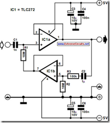
Input Impedance Booster II


The input resistance of a.c.-coupled op amp circuits depends almost entirely on the resistance with which the d.c. setting is determined. If CMOS op amps are used, the input resistance is normally high, currently up to 10 MΩ. If a higher value is needed, a bootstrap circuit may be used.
Impedance_Booster_Circuit_Diagram
This enables the input resistance to be boosted artificially to a very high value, indeed In the circuit shown in the diagram, resistor R1 sets the d.c. point for IC1a. The terminal of the resistor linked to pin 7 of IC1 would normally be at earth potential, so that the input impedance would be 10 MΩ. Connecting the other terminal of the resistor to earth via IC1a and network C2-R3-R2 as far as d.c. is concerned results in the requisite d.c. setting of the op amp.As far as alternating voltages are concerned, the input signal is fed back so that only a tiny alternating current flows through R1. Therefore, Rin=R1[(R2+R3)/R3]. With resistor values as specified, Rin is about 1 GΩ. One aspect must be borne in mind: the numerical value of (R2+R3)/R3 must not exceed 0.99. This means that the value of R3 cannot be less than 100 kΩ if the value of R2 is 10 MΩ. If these conditions are not met, the circuit will become unstable.
http://www.extremecircuits.net/2010/07/input-impedance-booster-ii.html