Custom Search

Thursday, September 23, 2010

4-Channel Commutator


To reach low channel ON resistance (<30 Ohm) and low OFF current leakage, 4-channel commutator uses the 2N4091. The DM7800 voltage translator is a monolithic device. This device give us +10V to -20V gate drive to the JFETs while at the same time giving DTL-TTL logic compatibility.

Here’s the circuit diagram:


Closed-Loop Automatic Power Control for RF Applications


This is a circuit of Closed-Loop Automatic Power Control for RF Applications. The circuit uses a log detector (AD8318) and a VGA (ADL5330). This circuit has a high temperature stability because of the high temperature stability of the AD8318. The AD8318 also ensures the same level of temperature stability at the output of the ADL5330 VGA. The ADL5330 is converted from an open-loop variable gain amplifier into a closed-loop output power control circuit by the log amp detector. The POUT vs. setpoint transfer function of AD8318 follows a linear-in-dB characteristic because the AD8318 has a linear-in-dB transfer function. Here is the circuit:

A sample of the output RF must be fed back to the detector by using additional attenuation and a directional coupler to operate the ADL5330 VGA in an AGC loop. A DAC is used to apply A setpoint voltage to the VSET input of the detector. The VOUT is connected to the GAIN pin of the ADL5330. The GAIN voltage is adjusted by the detector until the level at the RF input corresponds to the applied setpoint voltage. The correct balance between the setpoint voltage and the input signal level at the detector is set by the GAIN. [Source: Analog Devices Application Note]

555 IC Linear Ramp (Sawtooth) Generator/Oscillator


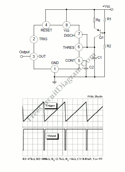
The Vc1 increases linearly when the pull-up resistor RA in the monostable circuit is replaced with constant current source, generating a linear ramp. The linear ramp generating circuit and the generated linear ramp waveforms illustration is shown in figures below.


Ic= (Vcc-Ve)/Re
Ve= Vbe + (R2/(R1+R2))Vcc
For example, if Vcc=15V, RE=20k, R1=5kW, R2=10k, and VBE=0.7V, VE=0.7V+10V=10.7V, Ic=(15-10.7)/20k=0.215mA
The current flowing through capacitor C1 becomes a constant current generated by PNP transistor and resistor when the trigger starts in a timer configured as shown in figure below.
Hence, the Vc is linear function. The gradient S of the linear ramp function is defined as:
S= (Vp-p)/T
The Vp-p is the peak to peak voltage. The Vc comes out as follows is the electric charge amount accumulated in the capacitor is divided by the capacitance.
V= Q/C
The above equation divided on both sides by T gives us
V/T= (Q/T)/C
and may be simplified into the following equation.
S=I/C
In other words, we can obtained the gradient of the linear ramp function appearing across the capacitor by using the constant current flowing through the capacitor. The gradient of the ramp function at both ends of the capacitor is S = 0.215m/0.022? = 9.77V/ms if the constant current flow through the capacitor is 0.215mA and the capacitance is 0.02uF. [Circuit's schematic diagram source: Philips Semiconductors Application Notes]

PID Controller Using Op-Amp


Generally, specifically combined ICs perform a control task. We can carry out simple controls using analog ICs, such as operational amplifier circuitry. The basic component of “Control Electronics” is an integrated circuit (IC). IC is a small electronic device made out of a semiconductor material.According to equation 1, this analog circuit calculates PID control response. Sensor signal VIN is amplified by IC1 (P mode), integrated by IC2 (I mode), and differentiated by IC3 (D mode), and all three modes are summed by IC4 to derive control response VOUT


[Source: Jeon and Chun]