
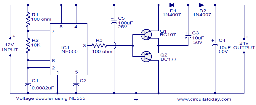
The circuit diagram of a very simple voltage doubler using NE555 timer is shown here. Here IC NE555 The negative terminal of the capacitor C3 will be shorted to ground through T2 and it will be charged to the input supply voltage. When the output of the astable multi vibrator is high, transistor Q1 will be ON and transistor Q2 will be OFF. The capacitor C4 will be charged to the voltage across capacitor C3 plus the input supply voltage (that is double the input voltage). This is how the circuit works.
This voltage doubler circuit can deliver only up to 50mA output current and above that current limit the output voltage will be dramatically reduced. The actual output voltage will be around 19V for a 12V DC input and also the output voltage will be a bit unstable. Anyway, for low current applications this circuit is well enough.